Transistor as an Amplifier – Circuit Diagram and Its Workings:
The main utility of a transistor lies in its ability of amplifying weak signals. The weak signal is applied at the input terminals and the amplified output is obtained across the output terminals. A transistor alone cannot perform the function of amplification and some passive components such as resistors and capacitors and a biasing battery is to be connected. Common emitter (CE) configuration, because of its high current, voltage and power gains, is much suited for most of the amplifier circuits. A common emitter N-P-N transistor as an amplifier circuit diagram is given in Fig. 10.32.
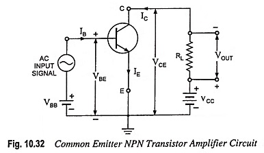
The weak signal is applied between emitter-base junction and output is taken across a load resistor RL connected in series with collector supply voltage VCC (Fig. 10.32). In order to obtain faithful amplification, it is necessary that the input circuit remains always forward biased regardless the polarity of the ac input signal. So a battery VBB is inserted in the circuit with the polarity indicated in addition to the signal voltage. This dc voltage is called the bias voltage and its magnitude is such as to keep the input circuit always forward biased regardless the polarity of the input signal.
The input circuit being forward biased has low resistance and a small change ΔVin in input signal voltage causes a relatively large change ΔIE in emitter current. This causes almost the same change in collector current because of transistor action. The collector current flowing through a high load resistance RL develops a large voltage across it. The change in output voltage across load resistance RL may be many times the change in input signal voltage. Thus voltage amplification A = ΔVout/ΔVin will be greater than unity, and the transistor acts as an amplifier. This is further illustrated below by considering typical circuit values.
Let the load resistance RL be of 10 kΩ and a change of 0.1 V in input signal voltage cause a change of 0.5 mA in emitter current.
This change of 0.5 mA in emitter current will also change collector current IC by approximately 0.5 mA. This change of 0.5 mA in collector current will produce a change of 0.5 x 10-3 x 10 x 103 i.e., 5 V in output voltage appearing across the load resistor RL of 10 kΩ. Thus the change of 0.1 V in input signal voltage causes a change of 5 V in the output voltage giving a voltage amplification of 5/0.1 = 50.
Necessity of Biasing: For most of the applications, transistors are required to operate as linear amplifiers (i.e., to amplify output voltage as a linear function of the input voltage). To achieve this, it is necessary to operate the transistor over region of its characteristic curves which are linear, parallel and equispaced for equal increments of the parameters. Such an operation can be ensured by proper selection of zero signal operating point and limiting the operation of the transistor over the linear portion of the characteristics. For proper selection of zero signal operating point, proper biasing i.e., application of dc voltages at emitter-to-base junction and collector-to-base junction is required.
If the transistor is not biased properly, it would work inefficiently and produce distortion in the output signal.