Junction Field Effect Transistor (JFET) – Construction, Symbols and Operation:
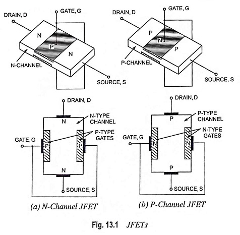
Depending upon the majority charge carriers, Junction Field Effect Transistor (JFET) have been classified into two types, namely (i) N-channel JFETs with electrons as the majority charge carriers and (ii) P-channel JFETs with holes as the majority charge carriers. N-channel JFETs are preferred because of mobility of electrons higher than that of holes. N-channel and P-channel FETs are shown in Figs. 13.1(a) and 13.1(b) respectively.
Basic Construction:
Its structure is quite simple. In an N-channel JFET an N-type silicon bar, referred to as the channel, has two smaller pieces of P-type silicon material diffused on the opposite sides of its middle part, forming P-N junctions, as illustrated in Fig. 13.1 (a). The two P-N junctions forming diodes or gates are connected internally and a common terminal, called the gate terminal, is brought out. Ohmic contacts (direct electrical connections) are made at the two ends of the channel—one lead is called the source terminal S and the other drain terminal D.
The silicon bar behaves like a resistor between its two terminals D and S. The gate terminal is analogous to the base of an ordinary transistor (BJT). It is used to control the flow of current from source to drain. Thus, source and drain terminals are analogous to emitter and collector terminals respectively of a BJT.
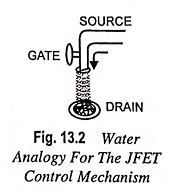
Analogies are seldom perfect and at times can be misleading, but the water analogy of Fig. 13.2 does provide a sense for the Junction Field Effect Transistor control at the gate terminal and the appropriateness of the terminology applied to the terminals of the device. The source of water pressure can be likened to the applied voltage from drain to source, which results in a flow of water (electrons) from the spigot (source). The “gate”, through an applied signal (potential) controls the flow of water (charge) to the “drain”, the drain and source terminals are at opposite ends of the N-channel as introduced in Fig. 13.1 because the terminology is defined for electron flow.
In Fig. 13.1 (a), the gate is P-region, while the source and the drain are N-regions. Because of this, a Junction Field Effect Transistor is similar to two diodes. The gate and the source form one of the diodes, and the gate and the drain form the other diode. These two diodes are usually referred to as the gate-source diode and the gate-drain diode. Since Junction Field Effect Transistor is a silicon device, it takes only 0.7 V for forward bias to provide significant current in either diode.
With the gate terminal not connected, and a potential applied (+ve at the drain and –ve at the source), a current called the drain current, ID flows through the channel located between the two P-regions. This current consists of only majority carriers – electrons in this case.
P-channel JFET is similar in construction to N-channel JFET except that P-type semiconductor material is sandwiched between two N-type junctions, as shown in Fig. 13.1 (b). In this case majority carriers are holes.
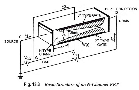
The basic structure of an N-channel JFET, together with the supply voltages, is shown in Fig. 13.3.
Standard Notations:
The noteworthy FET notations are as follows:
- Source: The terminal, through which the majority carriers enter the channel, is called the source terminal S and the conventional current entering the channel at S is designated as IS.
- Drain: The terminal, through which the majority carriers leave the channel, is called the drain terminal D and the conventional current leaving the channel at D is designated as ID. The drain-to-source voltage is called VDS, and is positive if D is more positive than S.
- Gate: There are two internally connected heavily doped impurity regions formed by alloying, by diffusion, or by any other method available to create two P-N junctions. These impurity regions are called the gate G. A voltage VGS is applied between the gate and source in the direction to reverse bias the P-N junction. Conventional current entering the channel at G is designated as IG.
- Channel: The region between the source and drain, sandwiched between the two gates is called the channel and the majority carriers move from source to drain through this channel.
Schematic Symbols:
The schematic symbols for N-type and P-type JFETs are shown in Figs. 13.4 (a) and 13.4 (b) respectively. The vertical line in the symbol may be thought as channel and source S and drain D connected to the line.
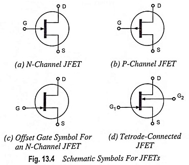
Note that the direction of the arrow at the gate indicates the direction in which the gate current flows when the gate junction is forward biased. Thus for the N-channel JFET, the arrow at the gate junction points into the device and in P-channel JFET, it is away from the device.
An alternative symbol for an N-channel JFET is shown in Fig. 13.4 (c). This symbol with its offset gate is preferred by many engineer and technicians. The offset gate points to the source end of the device, a definite advantage in complicated multistage circuit.
The symbol shown in Fig. 13.4 (d) is used where the terminals of the two gate regions are provided with separate connecting leads. In this case device is referred to as a tetrode-connected FET.
Polarity Conventions:
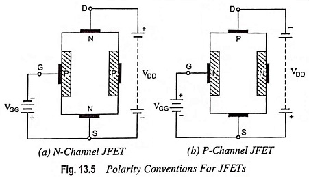
The polarities for N-channel and P-channel JFETs are shown in Figs. 13.5 (a) and 13.5 (b) respectively. In both of the cases the voltage between gate and source is such that the gate is reverse biased. This is the normal method of connection of Junction Field Effect Transistor. The drain and source terminals are interchangeable i.e. either end can be used as a source and the other end as a drain. The source terminal is always connected to that end of the drain voltage supply which provides the necessary charge carriers i.e. in an N-channel JFET source terminal, S is connected to the -ve end of the drain voltage supply for obtaining electrons whereas in P-channel JFET source terminal, S is connected to the +ve end of the drain voltage supply for getting holes.
Other noteworthy points are as follows :
- For N-channel JFET, ID and VDD are positive while VGG is negative.
- For P-cannel JFET, ID and VDD are negative while VGG is positive.
- Assumed positive directions of IS, ID and IG are into the JFET.
From the above statements it may be concluded that the action of a P-channel JFET is complementary, that is, all voltages and currents are reversed.
Operation of Junction Field Effect Transistor (JFET):
Let us consider an N-channel JFET for discussing its operation.
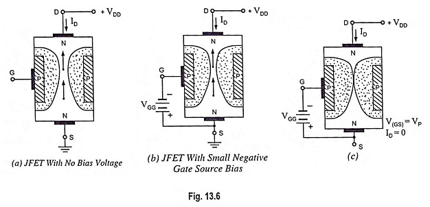
(i) When neither any bias is applied to the gate (i.e. when VGS = 0) nor any voltage to the drain w.r.t. source (i.e. when VDS = 0), the depletion regions around the P-N junctions are of equal thickness and symmetrical.
(ii) When positive voltage is applied to the drain terminal D w.r.t. source terminal S without connecting gate terminal G to supply, as illustrated in Fig. 13.6 (a), the electrons (which are the majority carriers) flow from terminal S to terminal D whereas conventional drain current ID flows through the channel from D to S. Due to flow of this current, there is a uniform voltage drop across the channel resistance as we move from terminal D to terminal S. This voltage drop reverse biases the diode. The gate is more negative with respect to those points in the channel which are nearer to D than to S. Hence, depletion layers penetrate more deeply into the channel at points lying closer to D than to S. Thus wedge-shaped depletion regions are formed, as shown in Fig. 13.6(a), when VDS is applied. The size of the depletion layer formed determines the width of the channel and hence the magnitude of current ID flowing through the channel.
To see how the width of the channel varies with the variation in gate voltage, let us consider the situation when the gate is biased negative with respect to the source while the drain is applied
with positive bias with respect to the source, as illustrated in Fig. 13.6 (b). Now the P-N junctions are reverse biased and depletion regions are formed. P-regions are heavily doped compared to the N-channel, so the depletion regions penetrate deeply into the channel. Since a depletion region is a region depleted of the charge carriers, it behaves as an insulator. The result is that the channel is narrowed, the resistance is increased and drain current ID is reduced. If the negative voltage at the gate is further increased, depletion layers meet at the centre and the drain current ID is cut off completely. On the other hand, if the negative bias to the gate is reduced, the width of the depletion layers gets reduced causing decrease in resistance and, therefore, increase in drain current ID. The gate-source voltage VGS at which drain current ID is cut off completely (pinched off), is called the pinch-off voltage VP. It is also to be noted that
- The amount of reverse bias is not the same throughout the length of the P-N junction. When the drain current flows through the channel, there is a voltage drop along its length. The result is that the reverse bias at the drain end is more than that at the source end making the width of depletion layer more at the drain end than that at the source end. Thus the channel becomes narrower at the drain end in comparison to that at source end, as shown in Fig. 13.6 (b).
- The channel is not completely closed at the drain end. Because in that case there will be no drain current, so there will be no voltage drop along the channel length and amount of reverse bias will become uniform and the wedge shaped depletion region will become rectangular one. The channel will open and the drain current will flow. However, at pinch-off voltage, the channel width is reduced to a constant minimum value to allow the flow of drain current.
- The N-channel JFET behaves as a vacuum tube triode. The drain and source perform the same functions as the plate and cathode, respectively and, like the grid of a triode, the Junction Field Effect Transistor gate controls the drain current. As is also the case with a grid, gate current is to be avoided, so the gate channel junctions are normally never forward biased.
The device is called the field-effect transistor (FET) because the drain current (output current) is controlled by the effect of the extension of the field associated with the depletion region developed by the reverse bias at the gate.
P-channel JFET operates in the same manner as an N-channel JFET except that channel current carriers will be the holes in place of electrons and the polarities of VGS and VDS are reversed.