Field Effect Transistor in Static Relay:
Field Effect Transistor in Static Relay is a unipolar device as compared to bipolar transistor already discussed. It consists of a bar of semiconductor material whose resistance is modulated by varying either the cross-sectional area of the bar or the density of current carriers in it, or both, by some electrical means. Two structures are used. One is an all-junction device in which the controlled modulation involves only the cross-section of the conducting channel. This is usually called junction FET. The other structure, called an insulated-gate FET (IGFET) or metal-oxide silicon FET (MOSFET) involves modulation of both the channel cross-section and the density of current carriers in it.
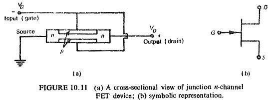
Junction FET is illustrated in cross-section in Fig. (10.11). An n-type bar of germanium is flanked by two regions of p-type germanium. The conduction current to be modulated is carried between the ends of n-type bar. The cross-sectional area available for conduction between the two p-type regions is a function of the magnitude of the reverse bias between the two p-type regions and the n-type bar. The input impedance of this device is quite high, and the output impedance is moderately high.
![]()
This type of device shows less internal feedback between the input and output than the conventional transistor. Typical characteristic curves of junction FET are shown in Fig. (10.12). It has characteristics similar to pentode tube. A few volts negative bias on the gate blocks the current between drain and source by virtue of the Field Effect Transistor in Static Relay.
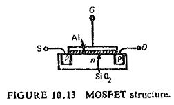
The MOSFET structure is shown in Fig. (10.13). Here it can be seen that two diffused p-regions, the source and drain are separated by the n-type material of the starting crystal. On top of this insulating oxide between the source and drain regions a metal gate electrode of aluminium is deposited. Aluminium contacts are also made to the source and drain regions. If a negative charge of several volts is placed upon the gate electrode, an equal positive charge will gather on the surface of the semiconductor crystal just beneath the oxide. This positive charge now connects the p-type source and drain regions, and since it is mobile it forms a thin conducting channel between them. It has a very high input impedance. The major advantage of the device is that the high input impedance is retained for either a positive or negative input voltage, since the gate is insulated from the rest of the structure by the SiO2 layer. This behavior contrasts with the junction FET where the gate is a reverse biased junction for one input polarity but a forward biased junction for the other input polarity.
The FET as a Switch:
At low frequencies the FET has no offset voltage. There is no threshold required of the signal being switched. In an ordinary bipolar transistor the signal being switched must exceed the voltage of the knee in the forward diode characteristic of the collector before there is appreciable signal through the switch in the on state. Here the channel, when opened by the gate, is a linear resistance requiring no such threshold. At a high frequency of switching there is a current due to the rapid charging and discharging of the gate capacitance through the channel, creating an IR drop in the channel which acts like an offset voltage.