Logic Circuit in Static Relay:
The concept of Logic Circuit in Static Relay can be better understood by considering the logic operations performed by the devices rather than the actual happenings that occur during their operation. This makes complex static relay operation also simple, because the interest then is only on what happens rather than how it happens, and the logic part of the operation is independent of devices used to realize the events dictated by the logic.
Basically, all relays are bistable devices, i.e. they have two stable states; either they operate or they do not operate. Consequently Boolean algebra can be applied to study and analyze protection schemes consisting of a number of relays. Using these techniques simplified block schemes can be drawn according to the logical functions performed by the various units.
In a d.c., or level-logic, system a bit is implemented as one of two voltage levels. The more positive voltage is the 1 level and the other is the 0 level, the system is said to employ d.c. positive logic. On the other hand, a d.c. negative logic system is one which designates the more negative voltage state of the bit as the 1 level and the more positive as the 0 level.
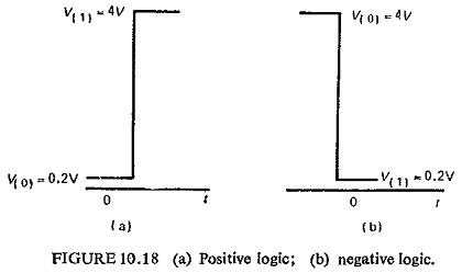
Figure (10.18) illustrates these two types of logic systems. Positive logic is usually followed.
Basic Operations:
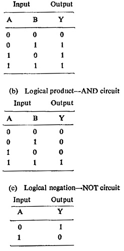
The three basic operations of Boolean algebra are
- Logical sum—OR circuit.
- Logical product—AND circuit.
- Negation—NOT circuit.
The output of an OR assumes the 1 state if one or more inputs assume the 1 state.
The output of an AND assumes the 1 state if and only if all the inputs assume the 1 state.
The output of a NOT circuit takes on the 1 state if and only if the input does not take on the 1 state.
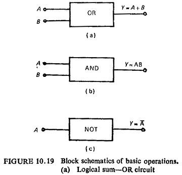
These basic operations are represented block schematically in Fig. (10.19) along with their truth table which contains a tabulation of all possible input values and their corresponding outputs. Different combinations of these circuits can result in other logic circuits such as NOR and NAND circuits.
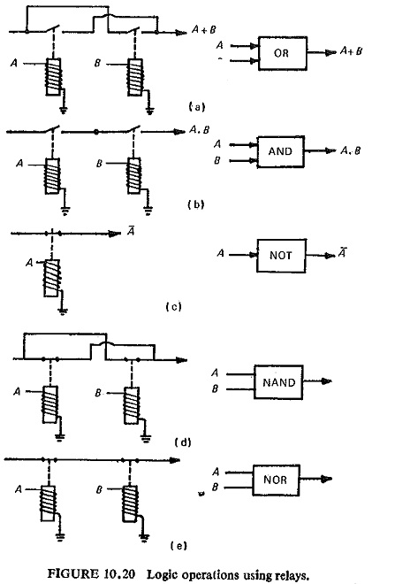
Relay Logic:
To start with, to make a connection between relay circuits and their logic operations, the basic operations mechanized using relays are shown in Fig. (10.20). All contacts are shown in their normal position, i.e. deenergized position. Thus each relay operation could be subdivided into basic switching functions which in turn can be represented by a suitable logic circuit.
In the following section, it will be shown that these logic circuits can be obtained using semiconductor devices such as diodes or transistors.
Diode Logic (DL):
The two stable states of the diode are conducting (i.e. forward bias) and nonconducting (i.e. reverse bias) states. Conventional diode OR gate (circuit) and AND gate are shown in Fig. (10.21).
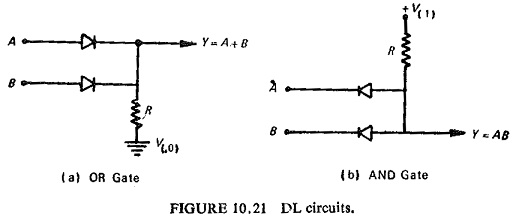
One of the disadvantages of diode logic is that negation cannot be performed using diodes and this is where transistors are helpful.
Transistor Logic:
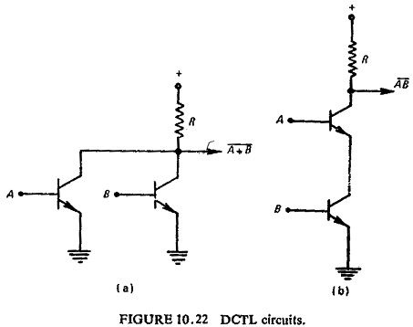
A number of logic circuits can be designed using transistors, specially because of the two types (npn and pnp types). Logic circuits using transistors could be developed in two forms, viz. resistor transistor logic (RTL) and direct coupled transistor logic (DCTL).
Basic NAND and NOR circuits based on the latter scheme (DCTL), are shown in Fig. (10.22).
The RTL class of circuits were developed to achieve improved stability of operation. In addition, it simplifies the general gate circuitry and does not require stringent control of transistor parameters. Commonly used RTL circuits are shown in Fig. (10.23).
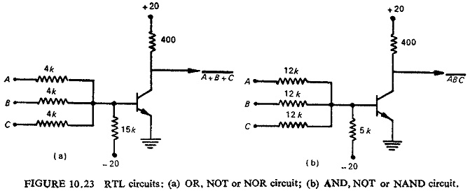
By using capacitances across the input resistors, the switching speed of the circuit can be increased. In such a case they are called resistance capacitance transistor logic (RCTL).