Explain Steady State Conditions in Semiconductor:
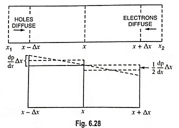
Explain Steady State Conditions in Semiconductor – When the P-N junction is forward biased, current flows quite freely P to N in a P-N junction, as discussed in Fig. 6.28. But when the P-N junction is reverse biased, there is virtually no flow of current. This asymmetry of the current flow makes the P-N junction diode very useful as a rectifying device. Biased P-N junctions can also be employed as voltage-variable capacitors, photocells, light emitters, and many more devices. Transistors and controlled switches can be formed by using two or more junctions.
In most P-N junctions Steady State Conditions, the space charge region is small compared with its area and the doping is normally moderate to heavy. This results in a small resistance in each neutral region and only a small voltage drop can be maintained outside the space charge region. The effects of bias on the important properties of the junction are depicted in Fig. 6.53.
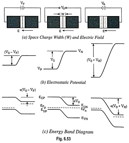
A forward bias (P positive w.r.t. N) raises the electrostatic potential on the P-side relative to the N-side. The electrostatic potential barrier at the junction is reduced due to forward bias to a lower value.
The opposite occurs for a reverse bias i.e. the electrostatic potential on P-side is reduced w.r.t. to N-side and the potential barrier at the junction becomes larger. The electric field in the space charge region decreases with forward bias, and increases with reverse bias because applied electric field opposes built-in field. The separation of the energy bands is directly related to the electrostatic potential barrier at the junction. The height of the electron energy barrier is equal to the electronic charge e times the height of the electrostatic potential barrier.
The shifting of the energy bands under bias means a separation of the Fermi energy levels on either side of the junction. In energy units of electron volts, the Fermi energy levels in the two neutral regions are separated by an energy eV numerically equal to the applied voltage V. Under forward bias the Fermi level on the N side EFn is above EFp by the energy eVF and for reverse bias EFp is eVR joules higher than EFn.
Majority carrier electrons on the N-side form the diffusion current which surmounts the potential energy barrier to diffuse to the P-side. The diffusion current is quite large under forward bias. More holes can diffuse from P to N under forward bias due to a lower bather. For reverse bias the barrier becomes very large and virtually no electrons in the N-side conduction hand or holes in the P-side valence band have enough energy to pass through it. In this case the diffusion current is negligible.
The drift current is not so sensitive to the height of potential barrier. This current is limited not by how fast carriers move down the barrier but rather how often. The electron drift current does not depend on how fast a single electron moves from P to N side but on how many electrons move down the barrier per second.
The hole and electron drift currents at the junction are independent of the applied voltage.
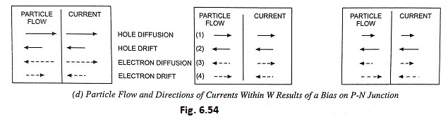
The total current across the junction consists of the sum of the diffusion and drift currents. As indicated in Fig. 6.54 electron and hole diffusion currents are from P to N, even though particle flow directions are opposite to each other and the drift currents are from N to P. The net current crossing the junction is zero at equilibrium. Under reverse bias both diffusion components are negligible. The current under equilibrium conditions is zero since the generation and diffusion currents balance each other.