Ebers Moll Model for PNP Transistor:
Device modelling aims at relating physical device parameters to device terminal characteristics. Device modelling is especially important for integrated circuits, since simple and accurate device models are required to predict the performance of a circuit. Generally, by making a model more accurate, we make it more complex. Thus, there is a trade-off between accuracy and complexity. Ebers Moll Model is a transistor model which describes the operating states of a transistor. This model is useful to obtain information about the dc characteristics of a transistor.
The transistor operates in active region when emitter junction is forward biased and collector junction is reverse biased. This model generalizes the behavior of a transistor by taking into account the inverted mode of operation of transistor.
The dependence of the currents in a transistor upon the junction voltages, or vice versa may be obtained by starting with Eq. (10.12), reproduced here
![]()
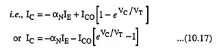
Subscript N to α has been added in order to indicate the normal operation of the transistor. Minus sign has been introduced with αNIE to take into account its direction.
In inverted mode of operation, equation corresponding to Eq. (10.17) may be written as
![]()
Here αI is the inverted common-base current gain, just as αN in Eq. (10.17) is the current gain in normal operation. IEO is the emitter-junction reverse saturation current, and VE is the voltage drop from P-side to N-side at the emitter junction and is positive for a forward-biased emitter.
Ebers Moll Model interpreting Eqs. (10.17) and (10.18) in terms of a circuit is given in Fig. 10.13 for a P-N-P transistor. It involves two ideal diodes connected back to back with reverse saturation currents –IEO and –ICO and two dependent current-controlled current sources shunting the ideal diodes. The current sources account for the minority-carrier transport across the base. By applying KCL to the collector node (Fig. 10.13), we have
Collector current,
![]()
where I is the diode current. As l0 is the magnitude of reverse saturation current, then l0 = -ICO. Substituting l0 = -ICO in above equation we have
Collector current,
![]()
which is nothing but the general expression for collector current of a transistor given in Eq. (10.17). Thus, this Ebers Moll Model is valid for both forward- and reverse-biased static voltages applied across the transistor junctions.
Here, base spreading resistance has been omitted and the difference between ICBO and lCO have also been neglected.
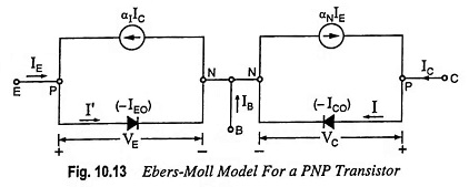
From Fig. 10.13 it is evident that dependent current sources can be eliminated from the figure provided αN = αI = 0. For example, by making the width of the base much larger than the diffusion length of the minority carriers in the base, all the minority carriers will recombine in the base and none will survive to reach the collector. In such a condition transport factor β and hence also current gain factor α will be zero. Thus under these conditions, the transistor action ceases, and we simply have two diodes placed back to back.
From the above discussion it is obvious that a transistor cannot be constructed by simply connecting two separate (isolated) diodes back to back.