Transistor Chopper Circuit:
Transistor Chopper Circuit – A single transistor used as a dynamic switch to convert low level dc signal to an ac waveform is shown in Fig. 14.34.
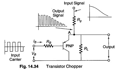
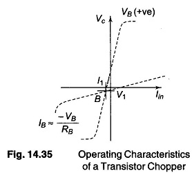
If the voltage applied to the transistor base is negative (in the case of a PNP transistor), both emitter and collector diodes are shorted, and the output voltage approximates V1 as shown in the Operating Characteristics of a Transistor Chopper Circuit Fig. 14.35. However, if a positive base voltage is applied to the chopping transistor (PNP), the diodes are open-circuit. The resistance from point A in Fig. 14.34 will then be in the Meg ohms range, and signal VB applied to the input of this circuit, is not attenuated.
Devices of this type use low drive power and have a good frequency response, but there is a leakage current. Since the junctions of a transistor are in physical contact with each other, there is a residual feed through of signals from the drive circuit to the output circuit, and such a minor signal may be interpreted by the following amplifier as a true input signal requiring amplification. If no voltage is applied at the composite system input, the voltage at point A (Fig. 14.34) during the high impedance portion of the cycle is approximately – I1 x (RgRL)/Rg + RΔ where RL is load resistance.
Some typical coordinates of point B (Fig. 14.35) are
![]()
Some of the temperature dependent drift of voltage V1 may be reduced by the use of two transistors whose connection scheme is shown in Fig. 14.36. The coordinate values of the matched silicon transistor may thereby made to remain between ± 0.2 mV dc and = ± 0.2 μA over a very wide temperature range. If Rg or RL is kept at a small value, undesired drift due to current I1 can be minimized.
![]()
In any chopper circuit, keeping the active chopper elements at constant temperature reduces drift. If two elements are used to cancel drift, it is important to keep the two at the same temperature, and a good way to prevent temperature drift is to make both elements a part of the same integrated circuit. This is done by the use of an integrated double emitter bipolar transistor.