Simple Biasing Circuit Diagram:
The simplest biasing circuit diagram could be as shown in Fig. 12.4.
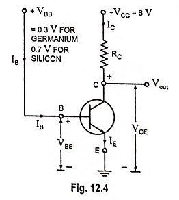
The emitter-base junction is forward biased by the battery VBB and the collector-base junction is reverse biased by the battery VCC. The voltage VBE across the forward biased junction is very low (0.3 V for Ge and 0.7 V for Si), therefore, the battery voltage VBB must also be of the same order.
The voltage VCC of battery required for reverse bias junction should be of a much large value than voltage VBB so as to reverse bias the collector-base junction. Since it is extremely difficult to have a battery of voltage as low as 0.3 V or 0.7 V, this is not a practical circuit.