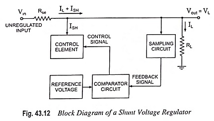
Shunt Voltage Regulator Block Diagram:
A shunt voltage regulator provides regulation by shunting current away from the load. The block diagram of such a voltage regulator is depicted in Fig. 43.12. The input unregulated voltage provides current to the load. Some of this current is shunted away by the control element to maintain the regulated output voltage across the load. If the output voltage tends to change due to change in load, the sampling circuit provides a feedback signal to a comparator circuit which then provides a control signal to vary the magnitude of current shunted away from the load. For example, when the output voltage tends to fall, the sampling circuit provides a feedback signal to the comparator circuit which then provides a control signal to draw lesser shunt current, providing more load current, thereby keeping the regulated voltage constant.
1. Transistor Shunt Voltage Regulator:
A shunt voltage regulator using an NPN transistor and a zener diode is shown in Fig. 43.13. A series resistance Rse is connected in series with the unregulated (or input), supply. Zener diode is connected across the base and collector terminals of the NPN transistor and the transistor is connected across the output, as shown in Fig. 43.13.
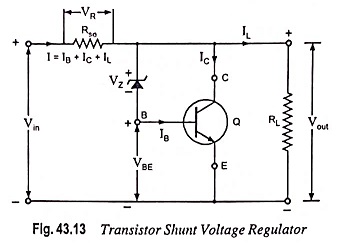
Unregulated voltage is reduced, due to voltage drop in series resistance Rse, by an amount that depends on the current supplied to the load RL. The voltage across the load is fixed by the zener diode and transistor base-emitter voltage VBE.
Output voltage is given as
![]()
Since both VZ and VBE remain nearly constant so output voltage Vout remains nearly constant. This is explained below:
If the input (or supply) voltage increases, it causes increase in Vout and VBE resulting in increase in base current IB and therefore, increase in collector current IC (IC = βIB). Thus with the increase in supply voltage, supply current I increases causing more voltage drop in series resistance Rse and thereby reducing the output voltage. This decrease in output voltage is enough to compensate the initial increase in output voltage. Thus output voltage remains almost constant. Reverse happens should the supply voltage decrease.
If the load resistance RL decreases, output current IL increases and this increase in output current is supplied by decrease in base and collector currents IB and IC. Thus the input current I remains almost constant causing no change in voltage drop across series resistance Rse. Thus output voltage Vout being the difference of supply voltage (fixed) and series resistor drop VR (fixed) remains constant. Reverse happens should the load resistance increase.
Limitations:
- There is considerable power loss in series resistor Rse.
- A large proportion of supply current I flows through the transistor rather than to load.
- There are problems of overvoltage protection in the circuit.
For the above reasons, a series voltage regulator is preferred over the shunt voltage regulator.
2. Improved Transistor Shunt Voltage Regulator:
An improved transistor shunt voltage regulator circuit is illustrated in Fig. 43.14. The zener diode provides a reference voltage in order that the voltage across R1 senses the output voltage. As the output voltage Vout tends to change, the current shunted by transistor Q1 is varied in order to maintain the output voltage constant. Transistor Q2 provides a larger base current to transistor Q1 than the circuit shown in Fig. 43.13, so that the regulator handles a larger load current. The output voltage is set by the zener voltage and that across the two transistor base emitters.
![]()
Limitations of Transistorized Power Supplies:
The stabilized voltage that can be obtained from transistorized power supplies is limited, to about 30-40 V only, because maximum safe value of VCE is about 50 V. This puts a limit to the use of transistorized power supplies.