Controlled Transistor Series Regulator or Negative Feedback Regulator:
A controlled transistor series regulator is shown in Fig. 43.6. This Controlled Transistor Series Regulator circuit is quite similar to that of a simple transistor series voltage regulator except that an additional transistor Q2 is inserted in the circuit. The emitter terminal of this transistor Q2 is connected to the negative terminal of input supply through a zener diode. The base of this additional transistor is connected to the variable tap of a potentiometer.
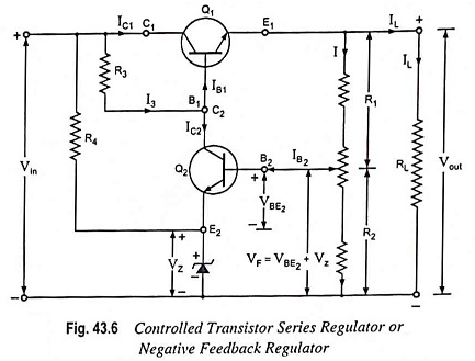
This voltage regulator employs the principle of negative feedback to hold the output voltage almost constant despite variations in supply voltage and/or load current. That is why this regulator is also called a negative feedback regulator.
Transistor Q1, the control element, is called the pass transistor because all the load current flows through it. Zener diode and resistor R4 act as a reference element. The voltage divider (or potentiometer) consisting of resistors R1 and R2 samples the output voltage and delivers a negative feedback voltage to the base of transistor Q2 and this feedback voltage (VF = VBE2 + Vz) controls the collector current of transistor Q2.
Operation:
Suppose the output voltage increases (due to any reason), the voltage across R2 is also increased as it is part of the output circuit. This causes an increase in voltage (VBE2 + Vz). As a result IB2 and also IC2 increases. Assuming I3 relatively constant, IB1 decreases. Decrease in base current of transistor Q1 causes the increase in collector-emitter resistance of transistor Q1. This causes an increase in VC1E1 thereby off-setting the increase in output voltage. Thus output voltage remains constant. Reverse happens should the output voltage decrease.
The voltage V2 provided by the potential divider R1-R2 must be equal to the sum of the base-emitter voltage of transistor Q2 and the zener diode i.e.,
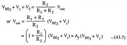
Thus the regulated output voltage is equal to the closed-loop gain multiplied by the sum of zener voltage and base-emitter voltage of transistor Q2 (the sensing element).
Limitations of Controlled Transistor Series Regulator:
Like emitter follower regulator this regulator also has the drawback of excessive power dissipation. Due to this high power dissipation output of the power supply is limited to 30-40 V, as safe value of VCE is 50 V.
Another drawback of this regulator is that it has no overload/short-circuit protection.