Two Stage CE Amplifier using Series Voltage Negative Feedback:
Negative Feedback Amplifier Circuit – A two-stage, capacitor-coupled BJT amplifier is shown in Fig. 13-10. This is the same Two Stage CE Amplifier circuit discussed already with the addition of feedback components RF2, RF1, and CF1. The output voltage is divided across RF2 and RF1 to produce a feedback voltage in series with the signal at the base of Q1. 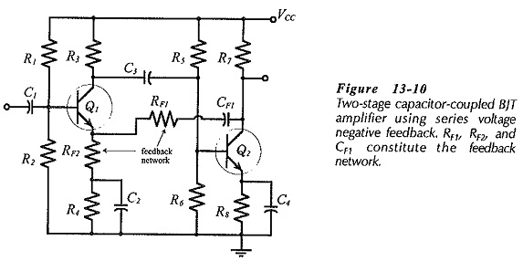
CF1 (in Fig. 13-10) is a dc blocking capacitor to prevent the dc voltage at Q2 collector from affecting the Q1 bias conditions. CF1 behaves as an open-circuit to do and a short-circuit to ac. Consequently, CF1 is not included in the mid-frequency no equivalent circuit of the feedback network in Fig. 13-11. Capacitor C2 behaves as a short-circuit at middle and higher frequencies, so C2 and R4 (shorted by C2) are also absent from the mid-frequency no equivalent circuit.
The signal voltage (vs) is applied between Q1 base and ground, as illustrated in Fig. 13-11, and the output voltage (vo) is developed between Q2 collector and ground. The feedback voltage (vf) is developed across resistor RF2, between the Q1 emitter terminal and ground. The input voltage (vi) appears across the Q1 base-emitter terminals as the difference between vs and vf.
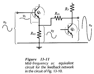
From previous topics of a Two Stage CE Amplifier, it is known that the circuit output voltage is in phase with the signal voltage. When the instantaneous level of vs is positive-going, vo is also positive-going, and consequently vf is in phase-opposition with vs. When vs goes up (positively), vf also goes up, and consequently, the voltage (vi) at the base-emitter of Q1 is reduced from vs to,
![]()
Note that the Q1 bias resistors (R1 and R2) in Fig. 13-10 are outside the feedback loop, and are unaffected by feedback. The impedance looking-into the transistor base is within the feedback loop, so it is altered by feedback. Also, recall that the Q2 collector resistor (R7) is unaffected by negative feedback, and that the impedance looking-into the transistor collector terminal is changed by negative feedback.
The feedback factor for the circuit in Figs. 13-10 and 13-11 is,
From Eq. 13-3,
Usually RF1 ≫ RF2, so
Negative Feedback Amplifier Design:
A Two Stage CE Amplifier using Series Voltage Negative Feedback amplifier like the one shown in Fig. 13-12, is best designed first as an amplifier without feedback. The feedback component values are then determined, and the circuit is modified as necessary.
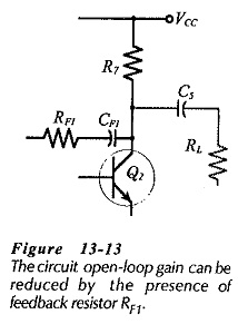
Like RL, RF1 is an additional load at the collector of the second stage in Fig. 13-12. As illustrated in Fig. 13-13, the voltage gain of the second stage is proportional to the total load (RL||R7||RF1), consequently, RF1 has the effect of reducing the second stage gain. A large open-loop gain is required for good gain stability, so RF1 should be selected as large as possible.
Resistor RF2 is an unbypassed resistor in series with the emitter of Q1. As such, it would seem to reduce the first stage voltage gain, and thus reduce the circuit open-loop gain. However, because vf is applied to Q1 emitter, the effective open-loop gain is the voltage gain from the BE terminals of Q1 to the collector of Q2. So, RF2 does not alter the overall open-loop gain. (RF2 is omitted when calculating the circuit open-loop gain.)
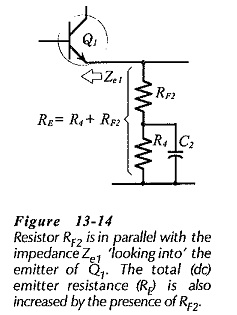
Another consideration for RF2 is that it is in parallel with the impedance (Ze1) at the emitter of Q1, (see Fig. 13-14). Without negative feedback, Ze1 would usually equal the transistor hib, value, which is typically 26 Ω when IC = 1 mA. With negative feedback, Ze1 can be shown to range from about 2.5 kΩ to 30 kΩ depending upon Av and B. Resistor RF2 should be selected much smaller than Ze1. However, RF2 should be as large as possible to give the largest possible value for RF1; (from Eq. 13-10, RF1 ≈ ACL X RF2).
A reasonable starting point for feedback network design is to select RF2 much lower than Ze1/10: in the range of 100 Ω to 470 Ω. RF2 could also alter the dc bias conditions for Q1. Consequently, it might be necessary to reduce R4, so that R4 and RF2 add up to the original resistance selected for R4 (or RE), (see Fig. 13-14).
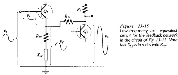
Figure 13-15 shows a low-frequency ac equivalent circuit for the feedback network. Note that capacitor CF1 is still taken as an ac short circuit, so XCF1 is assumed to be very much smaller than RF1. The impedance of capacitor C2 is show, and because XC2 is assumed to be very much smaller than resistor R4, R4 is omitted.
From Fig. 13-15, vo is divided across RF1 and (RF2 + jXC2) to give vf, so the feedback factor is,
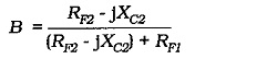
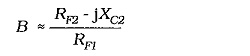
Assuming that (RF2 – jXC2) ≪ RF1,
From Eq. 13-3,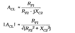
When XC2 = RF2,
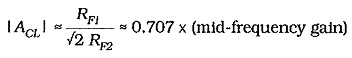
To set a desired frequency lower cutoff frequency (f1),
![]()
As already mentioned, XCF1 must be very much smaller than RF1 at the low cutoff frequency for the amplifier. It can be shown that, if XCF1 = RF1 at f1, the closed-loop gain would actually increase at frequencies below f1. CF1 is normally calculated from,
![]()
Capacitor CF1 can often be eliminated. If RF1 is large enough, direct connection of RF1 from Q2C to Q1E in Fig. 13-12 will have a negligible effect on the circuit bias conditions. In fact, with a direct-coupled circuit, direct connection of the feedback resistors might enhance the circuit bias stability.
The circuit input impedance is increased by negative feedback, so input coupling capacitor C1 can be recalculated as a smaller capacitor, (XC1 = Zin/10 at f1). Recall that the bias resistors are not affected by feedback. Regardless of how high the circuit input impedance might become, C1 should normally be selected as a minimum of 0.1 μF, to ensure that it is much larger than any stray capacitance at the circuit input.
The emitter bypass capacitor C4 (in Fig. 13-12) was calculated to have XC4 = 0.65 hib2 at f1. So, XC4 will reduce the circuit open-loop gain (Av) at f1. However, even with this gain reduction. Av should still be much larger than ACL, so C4 can normally be left as calculated for an amplifier without feedback.
Recall from earlier discussion that, when designing an amplifier without feedback, the collector resistor (RC2) for the output transistor is usually selected as equal to, or less than, RL/10. This is because without negative feedback Zo ≈ RC2. Negative feedback normally reduces Zo to a value much smaller than RC2. So, RC2 does not have to be selected as RL/10 when designing a Two Stage CE Amplifier using Series Voltage Negative Feedback. Instead, any convenient level of VRC and IC can be used for calculating a suitable RC2 value.