Equilibrium Conditions in Semiconductor Physics:
The electron and hole concentrations, under thermal Equilibrium Conditions can be found by knowing the position of the Fermi energy EF with respect to the bottom of the conduction band energy EC and top of valence band energy EV. As discussed already, in case of an intrinsic semiconductor, the Fermi level lies midway between the conduction and valence bands.
With the rise in temperature above 0 K, the valence electrons gain thermal energy. A few electrons in the valence band may gain sufficient energy to jump to the conduction band. Under this Equilibrium Conditions an empty state or hole is generated in the valence band. In an intrinsic semiconductor electrons and holes are generated in pairs by thermal energy so that the number of electrons in the conduction band is equal to the number of holes in the valence band.
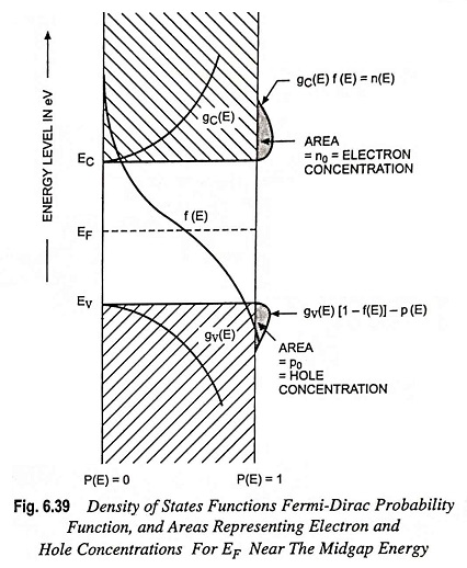
Figure 6.39 shows a plot of the density of states function in the conduction band gC(E), and the density of states function in the valence band gV(E), and the Fermi-Dirac probability function for T > 0 K when EF is approximately halfway between EC and EV.
Contact Potential:
Upon joining the two regions P and N (Fig. 6.37) holes diffuse from P-region to N-region and electrons diffuse from N-region to P-region, as discussed already. The resulting diffusing current cannot build up indefinitely due to creation of opposite electric field at the junction. The electric field E builds up to the point where the net current is zero at equilibrium. The electric field appears in some region W about the junction, called the transition region, and there is an equilibrium potential difference V0 across W, called a contact potential.
The contact potential across W is a built-in potential barrier, essential to the maintenance of equilibrium at the junction. The valence and conduction energy bands, are higher on the P-side of the junction than on the N-side by an amount eV0.
The relations between different quantities under conditions of equilibrium are:
The relationship between hole currents is
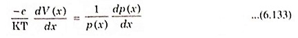
which can be simplified as
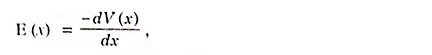
where the x-direction is arbitrarily taken from P to N. The electric field can be written in terms of the gradient in the potential,
so that Eq. (6.132) becomes
With the use of Einstein relation for μh/Dh, the integration of above Eq. (6.133) provides
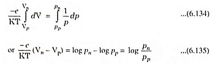
The potential difference Vn – Vp is the contact potential Vo. In terms of the equilibrium hole concentrations on either side of the junction
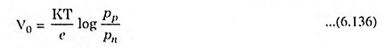
If a step junction is made up of material with NA acceptors/cm3 on the P-side and a concentration of ND donors on the N-side, Eq. (6.136) becomes
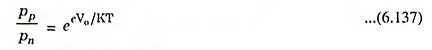
For the equilibrium conditions ppnp = n2i = pnnn, the above Eq. (6.137) becomes
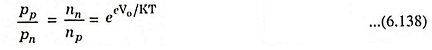
The above relation will be very useful in determination of I-V characteristics of the junction.