DC Load Line Analysis of Semiconductor Diode:
Figure 2-13(a) shows a DC Load Line Analysis of Semiconductor Diode in series with a 100 Ω resistance (R1) and a supply voltage (E). The polarity of E is such that the diode is forward biased, so a diode forward current (IF) flows. As already discussed, the circuit current can be determined approximately by assuming a constant diode forward voltage drop (VF). When the precise levels of the diode current and voltage must be calculated, graphical analysis (also termed DC Load Line Analysis of Semiconductor Diode) is employed.
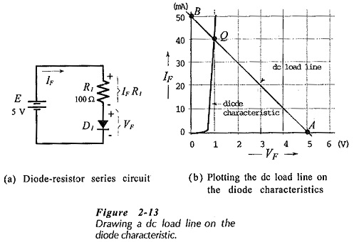
For graphical analysis, a dc load line is drawn on the diode forward characteristics, [Fig. 2-13(b)]. This is a straight line that illustrates all dc conditions that could exist within the circuit. Because the load line is always straight, it can be constructed by plotting any two corresponding current and voltage points and then drawing a straight line through them. To determine two points on the load line, an equation relating voltage, current,and resistance is first derived for the circuit. From Fig. 2-13(a),
![]()
Any convenient two levels of IF can be substituted into Eq. 2-3 to calculate corresponding VF levels, or vice versa.
Q Point:
The relationship between the diode forward voltage and current in the circuit in Fig. 2-13(a) is defined by the device characteristic. Consequently, there is only one point on the dc load line where the diode voltage and current are compatible with the circuit conditions. That is point Q, termed the quiescent point or dc bins point, where the load line intersects the characteristic. This may be checked by substituting the levels of IF and VF at point Q into Eq. 2-3. From the Q point on Fig. 2-13(b), IF = 40 mA and VF = 1 V. Equation 2-3 states that E = (IF R1) + VF. Therefore,
![]()
So, with E = 5 V and R1 = 100 Ω, the only levels of IF and VF that can satisfy Eq. 2-3 on the diode characteristics in Fig. 2-13(b) are IF = 40 mA and VF= 1 V.
Note that, although VF = 0 and VF = 5 V were used when, drawing the dc load line, no functioning semiconductor diode would have such forward voltage drops. These are simply convenient theoretical levels for constructing the DC Load Line Analysis of Semiconductor Diode.
Calculating Load Resistance and Simply Voltage:
In a diode series circuit [see Fig. 2-14(a)), resistor R1, indicates the slope of the dc load line, and supply voltage E determines point A on the load line. So, the circuit conditions can be altered by changing either R1 or E.
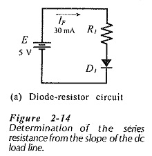
When designing a diode circuit, it may be required to use a given supply voltage and set up a specified forward current. In this case, points A and Q are first plotted and the load line is drawn. R1 is then calculated from the slope of the load line. The problem could also occur in another way. For example, R1 and the required IF are known, and the required supply voltage is to be determined. This problem is solved by plotting point Q and drawing the load line with slope 1/R1. The supply voltage is then read at point A.