Transistor Load Line Analysis (DC and AC Load Line and Q Point):
The concept of Transistor load line analysis is very important in understanding the working of a transistor. It is defined as the locus of operating point on the output characteristic of the transistor. It is the line on which the operating point moves when ac signal is applied to the transistor.
DC Load Line:
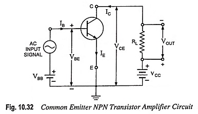
In the circuit shown in Fig. 10.32, VCC is the supply voltage to collector, RC (or RL) is the collector resistance (or load resistance) and VCE is the collector-to-emitter voltage. Applying Kirchhoff’s second law to the output or collector circuit we have,
This equation is to be plotted on the output characteristic of the transistor, VCE and lC are variables.
Identify this equation as y = mx + c where m = -1/RC as the slope of the line and IC = VCC/RC as intercept of the line on vertical current axis (Fig. 10.33).
Consider the following two particular situations:
![]()
By joining these two points A and B, dc load line is obtained. The dc load line represents the dynamic characteristic of the device. The dc load line provides the values of collector current IC and collector-emitter voltage VCE corresponding to zero signal conditions.
Quiescent Point:
It is a point on the dc load line which represents dc collector-emitter voltage VCE and collector current IC in the absence of ac signal. It is also called the operating point because the variations in VCE and IC take place about this point when signal is applied. The best position for this point is midway between cutoff and saturation points where VCE = 1/2 VCC. Point Q is quiescent point marked on the output characteristics shown in Fig. 10.33.
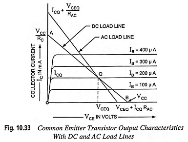
Selection of the operating point is done as per application for which the device is to be used. For example in case of a small signal amplifier, in which power is conserved, operating point is selected so as to provide lowest quiescent value of lC, while for an amplifier operated to deliver small amount of power, operating point is selected so that available quiescent current is about one-half of the maximum permissible collector current lC.
AC Load Line:
When an ac signal is applied, the transistor voltage VCE and collector current lC vary above and below the quiescent point Q. So point Q is common to both dc and ac load lines. The ac load line provides the values of VCE and IC when an ac signal is applied. For drawing ac load line, take a convenient collector current change ΔIC and compute the corresponding collector-emitter voltage change ΔVCE = -ΔIC.RC to obtain another point lying on the ac load line. Now the ac load can be drawn by joining this point and point Q. AC load is steeper than dc load line but the two lines intersect at the quiescent point Q determined by the biasing dc voltages and currents. AC load line takes into account the ac load resistance while the dc load line considers only the dc load resistance.