What is Transistor Transistor Logic (TTL) Circuit?
Texas instruments introduced transistor transistor logic (TTL), a widely used family of digital devices in 1964. It is fast, inexpensive and easy to use. Transistor Transistor Logic family consists of variety of SSI and MSI chips, with the help of that all kinds of digital circuits and systems can be built up.
The basic Transistor Transistor Logic circuit is the NAND gate. The circuit diagram is shown in Fig. 47.3.
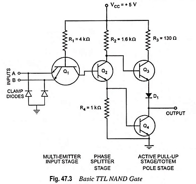
It can be seen that transistor Q1 has two emitters so it has two emitter-base junctions which can be used to turn transistor Q1 on. Up to eight emitters can be used in a multiple-emitter input transistor for an eight-input NAND gate. Other special feature of this circuit is totem-pole arrangement made by transistors Q3 and Q4 on the output side of the circuit.
Protecting diodes connected in multiple-emitter transistor protect the transistor from damage due to excessive input voltages.
Now let us have a look on the circuit operation. In the circuit diagram resistance R1 and transistor Q1 act like a 2-input AND gate. Transistor Q2 acts like an inverter, which inverts the output of transistor Q1 and hence the circuit operates like a NAND gate. Transistors Q3 and Q4 form a totem-pole connections at the output stage, either Q3 or Q4 is on at a time. When Q3 is on, the output is high; when Q4 is on, the output is low.
Now consider a case when both inputs A and B, are high. Emitter diodes of Q1 stop conducting and collector diode gets forward biased. With this base of transistor Q2 becomes high and it starts conducting. So a potential drop occurs across resistance R4, and base of transistor Q4 becomes high. So transistor Q4 becomes saturated and gives low output.
Consider the other case also, when both inputs or either is low, then base of Q1 becomes approximately at 0.7 V which reduces the base voltage of Q2 at almost zero volt, therefore, transistor Q2 is cut off. Almost no current flows through resistances R2 and R4 and, therefore, base voltage of Q4 becomes zero and Q4 is cut off. Base voltage of Q3 becomes high and since Q3 acts as an emitter follower, it produces high output.
The function of diode D1 is to prevent even the slight conduction of Q3, when the output is low. Voltage drop across the diode D1 keeps the emitter diode of Q3 reverse biased and so only Q4 conducts during the low output condition.
Totem-pole transistors are used to get low output impedance. During high output state Q3 conducts and provides output impedance of 70 Ω. During low output state, Q4 gets saturated and provides output impedance of approximately 12 Ω. So in both states, output impedance is low and it ensures that output voltage changes its value from one state to another quickly because stray capacitance is rapidly charged or discharged through low output impedance.
The fan-out in TTL totem-pole circuit is limited by the amount of current that the output transistor can sink in LOW state or can source in HIGH state.
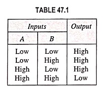
Function table for the two-input Transistor Transistor Logic NAND gate is given in Table 47.1.