Integrated Injection Logic (IIL or I2L) Circuit:
It is the latest entry into the bipolar saturated logic field. It uses no biasing and loading resistors at all. Resistors require lot of power and space on an IC chip. Hence, their elimination results in higher density circuits operating at much reduced power. Because of its high speed and less power dissipation, it is used in large computers. Another feature of Integrated Injection Logic (IIL or I2L) Circuit is that it is easy to fabricate.
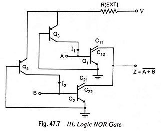
The circuit, as depicted in Fig. 47.7, consists of multiple collectors with a common base and emitter. The base current is provided by another transistor built in the chip.
Q1 and Q2 are multiple collector transistors and Q3 and Q4 act as current sources instead of resistors as in RTL. The base of Q3 and emitter of Q1 are tied, so also the collector and base, so that it makes for small area on the chip.
When supply voltage V is connected to emitters of Q3 and Q4, current is supplied to base of Q1 and Q2. The working of the Integrated Injection Logic (IIL or I2L) gate is explained below.
Case I : Both A and B LOW : A low at A will bypass the injected current from Q3 and make Q1 off. The input source acts as a sink for the current I1. Similarly Q2 will be off because input B is also low. Voltage at Z will be high.
Case II : Either A or B HIGH or Both HIGH : Current I1 or I2 or both are diverted to BE junctions of transistors Q1 and Q2 and they are turned on. The voltage at Z will be low being saturated voltage of 0.2 V. Thus a NOR output is obtained.
It may be noted that the current injection transistors Q3 and Q4 are PNP transistors whereas Q1 and Q2 are NPN type. This makes ease of manufacture and high packing density. The collector is relatively lightly doped, the base doped more heavily and emitter doped very heavily.