Zero bias PN junction:
Zero bias PN junction – Here we will examine the properties of the step junction in thermal equilibrium, where no currents exist and no external excitation is applied. We will determine built-in potential barrier through the depletion or space-charge region, electric field and width of the space-charge region.
Built-in Potential Barrier:
When no voltage is applied across the P-N junction (i.e., with zero applied bias), the junction is in the thermal equilibrium—the Fermi energy level is constant throughout the entire specimen. The valence and conduction bands energies have to bend while moving through the space-charge region because the relative position of these bands with respect to the Fermi energy changes between P and N regions.
Electrons in the conduction band of the N-region face a potential barrier when moving into the conduction band of the P-region. This potential barrier is known as the built-in potential barrier and is denoted by Vbi or V0. The built-in potential barrier maintains equilibrium between majority carrier electrons in the N-region and minority carrier electrons in the P-region. It also maintains equilibrium between majority carrier holes in the P-region and minority carrier holes in the N-region. This potential difference across the junction cannot be measured with a voltmeter as new potential barriers are being formed between the semiconductor and the probes which will cancel built-in potential barrier Vbi. As the condition pertains to equilibrium so no current is caused by this voltage.
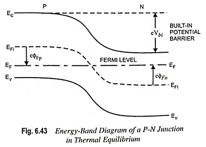
The intrinsic Fermi level is equidistant from the conduction band edge through the junction, as illustrated in figure. The built-in potential barrier Vbi is the difference between the intrinsic Fermi levels of the N and P-regions.
![]()
The electron concentration in the N-region conduction band,
![]()
where EFi and ni are the intrinsic Fermi energy and intrinsic carrier concentration, respectively.
Potential ΦFn in the N-region is defined as
![]()
Taking natural log of both sides of Eq. (6.146), setting no = ND we have
![]()
Similarly for the P-region,
The built-in potential barrier for the step junction is then
where VT is defined as the thermal voltage and is equal to k′T/e.
Electric Field:
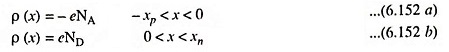
The separation of positive and negative space charge densities results in an electric field in a depletion region. Figure 6.44 depicts the volume charge density distribution in Zero bias PN junction assuming uniform doping and assuming an abrupt junction approximation.
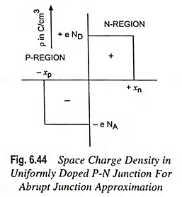
Let us assume that the space charge region abruptly ends in the N-region at x = + xn and at x = – xp (xp is a positive quantity) in the P-region.
The electric field is found from Poisson’s equation and is
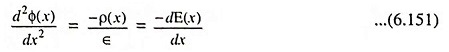
where Φ(x) is the electric potential, E(x) is the electric field, ρ(x) is the volume charge density and ∈ is the permittivity of the semiconductor material.
From Fig. 6.44, the charge densities are
Integrating Eq. (6.151), we find electric field in the P-region. We have
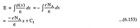
where C1 is a constant of integration.
The electric field is assumed to be zero in the neutral P-region for x < – xp as in thermal equilibrium the currents are zero. Since there are no surface charge densities within the Zero bias PN junction structure, the electric field is a continuous function. The constant of integration can be found by setting E = 0 at x = – xp.
So C1 comes out to be -eNA/∈ xp and electric field in the P-region is given by
![]()
The electric field in the N-region can be found from
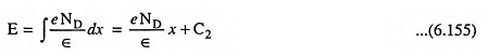
where C2 is another constant of integration which can be determined by setting E = 0 at x = xn, because the E-field is assumed to be zero in the N-region and is a continuous function. Thus we have
![]()
The electric field is also continuous at the metallurgical junction, or at x = 0. Equating Eqs. (6.154) and (6.156) at x = 0 we have
![]()
Above Eq. (6.157) reveals that number of negative charges per unit area in the P-region and number of positive charges per unit area in the N-region are equal.
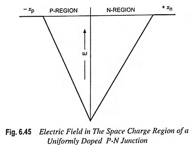
Electric field in the depletion region is depicted in Fig. 6.45. The electric field acts in direction from N to P-region, or in the negative x direction for this geometry. For the uniformly doped P-N junction, the E-field varies linearly with the distance through the junction and the maximum (magnitude) electric field is at the metallurgical junction. Though no voltage is applied between the P and N-regions but there is an electric field in the depletion region.
Integration of electric field gives potential in the junction. In the P-region, we have
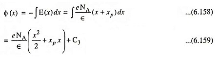
where C3 is again a constant of integration. The pd through the P-N junction is the important parameter, rather than the absolute potential. Let us set the potential equal to 0 arbitrarily at x = -xp. The constant of integration comes out to be
Thus the expression for potential in the P-region becomes
![]()
Integration of electric field in the N-region gives expression for the potential in the N-region and we have
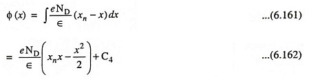
where C4 is a constant of integration. Setting Eqs. (6.160) and (6.162) equal at the metallurgical junction, or at x = 0 (because potential is a continuous function), we have
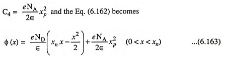
A plot of potential through the junction is depicted in Fig. 6.46. It shows the quadratic dependence of potential on the distance x.
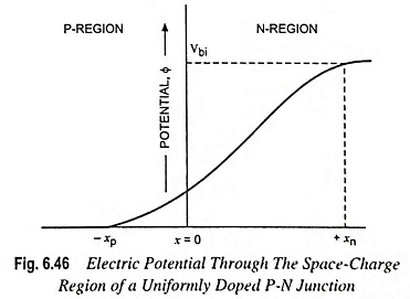
The magnitude of the potential at x = xn is equal to the built-in potential barrier Vbi, Eq. (6.163) yields.
![]()
The potential energy of an electron is given as E = – e Φ. It means that the electron potential energy also varies as a quadratic function of distance through the space charge region.
Space Charge Width:
The space charge region extends into the N and P-regions from the metallurgical junction. This distance is known as the space charge width.
Substituting Eq. (6.165) in Eq. (6.164) and solving for xn, we have
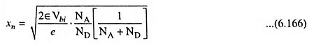
The above Eq. (6.166) provides the space charge width, or the width of the depletion region xn extending into N-region when the no voltage is applied between the P and N-regions.
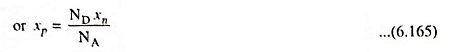
Similarly, if we solve for xn from Eq. (6.157) and substitute into Eq. (6.164), we have
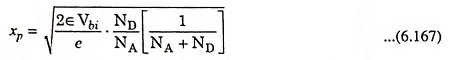
Total depletion or space charge width,
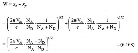
The built-in potential barrier can be determined from Eq. (6.150) and then the total space charge region width can be determined from above Eq. (6.168).