Basic Structure of PN Junction in Semiconductor:
Most semiconductor devices employ one or more P-N junctions. The P-N junction is the control element for the performance of all semiconductor devices such as rectifiers, amplifiers, switching devices, linear and digital integrated circuits. The PN Junction in Semiconductor is produced by placing a layer of P-type semiconductor next to the layer of N-type semiconductor. The interface separating the N and P regions is referred to as the metallurgical junction.
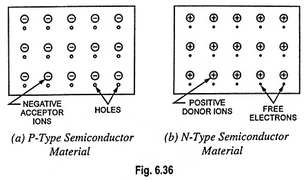
Figure 6.36 represents two blocks of semiconductor material, one P-type, and the other N-type. The P-type semiconductor block has mobile holes (shown by small circles) and the same number of fixed negative acceptor ions (shown by encircled minus sign). Similarly the N-type semiconductor block has mobile or free electrons (shown by dots) and the same number of fixed donor positive ions. Normally the holes, which are the majority charge carriers in P-type of material, are uniformly distributed throughout the volume of that material. Similarly the electrons, which are the majority charge carriers in N-type of material, are uniformly distributed throughout the volume of that material. Each region is electrically neutral because each of them carries equal positive and negative charges.
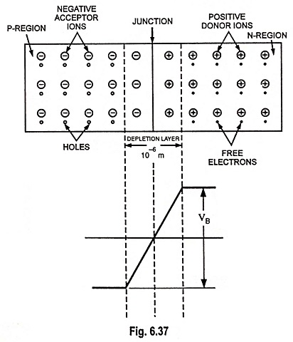
On the formation of PN Junction in Semiconductor some of the holes from P-type material tend to diffuse across the boundary into N-type material and some of the free electrons similarly diffuse into the P-type material, as illustrated in Fig. 6.37. This happens due to density gradient (as concentration of holes is higher on P-side than that on N-side and concentration of electrons is higher on N-side than that on P-side). This process is known as diffusion and current produced because of diffusion process is known as the diffusion current ID. The potential distribution diagram is shown in Fig. 6.37. From Fig. 6.37, it is obvious that a potential barrier VB or V0 is developed which results in an electric field. This field prevents the respective majority carriers from crossing the barrier region.
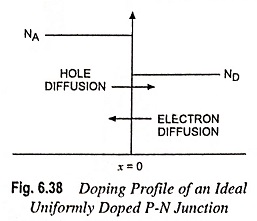
The doping profile of an ideal uniformly doped PN Junction in Semiconductor is depicted in Fig. 6.38.
It is evident that the free electrons crossing the junction create negative ions on the P-side by giving some atoms one more electron than their total number of protons. The electrons also leave positive ions (atoms with one fewer electron than the number of protons) behind them on the N-side. As negative ions are created on the P-side of the junction, the P-side acquires a negative potential. Similarly, the positive ions are created on the N-side and the N-side acquires a positive potential. The negative potential on the P-side prevents the migration of any more electrons from the N-type material to the P-type material. Similarly, the positive potential on the N-side prevents any further migration of holes across the boundary. Thus, the initial diffusion of charge carriers creates a barrier potential at the junction. The magnitude of barrier potential V0 is of the order of few tenths of a volt (0.3 V in case of Ge and 0.7 V for Si).
The region around the junction is completely ionised. As a result, there are no free electrons on the N-side, nor holes on the P-side. The region around the junction is termed as depletion region because the mobile charge carriers (i.e., free electrons and holes) have been emptied in this region.
Barrier Potential and Temperature:
Barrier voltage depends on doping density, electronic charge and temperature. For a given junction, the first two factors are fixed, thus making barrier potential dependent on temperature.
The junction temperature is the temperature inside a diode, right at the PN Junction in Semiconductor. The ambient temperature which is the temperature of air outside the diode, is different. In the conducting state, the temperature of the junction is higher than ambient temperature owing to heat dissipation by the recombination.
As mentioned above, the barrier potential depends on the junction temperature. An increase in junction temperature results in generation of more and more electrons and holes in doped regions. With the diffusion of these charges into the depletion layer, it becomes narrower i.e., barrier potential is reduced with the increase in junction temperature. It is found that for either silicon or germanium diodes, the barrier potential decreases 2 mV for each Celsius degree rise.