Terminal Characteristics of Junction Diodes:
The volt-ampere characteristic of a silicon junction diode is depicted in Fig. 7.14. The same Terminal Characteristics of Junction Diodes is depicted in Fig. 7.15 with some scales expanded and others compressed to reveal details—the changes in scale have resulted in the apparent discontinuity at the origin.
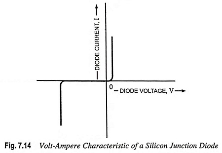
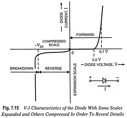
As shown in the figure, the Terminal Characteristics of Junction Diodes curve consists of three distinct regions :
- The forward-bias region, determined by V > 0.
- The reverse-bias region, determined by V < 0.
- The breakdown region, determined by V < – VZK.
The above three regions of operation are described below :
Forward-Bias Region:
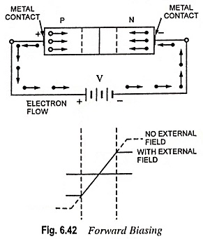
A positive value of current I means the current flowing from the P-region to the N-region. The diode is forward biased if the applied voltage V is positive i.e., P-side is connected to the positive terminal and N-side is connected to negative terminal as shown in Fig. 6.42.
The current flowing through the junction diode is given by Eq. (7.20).
![]()
In Eq. (7.20) I0 is a constant for a given diode at a given temperature. A formula for I0 in terms of the temperature will be given in Art. 7.10. The current I0 is usually called the saturation current, and sometimes denoted by Is. Another name for the saturation current is the scale current. This name arises from the fact that I0 is directly proportional to the cross-sectional area of the diode. Thus doubling of junction area results in a diode with double the value of I0 and, as the diode equation indicates, double the value of current I for a given forward voltage V. For “small-signal” diodes (small size diodes intended for low-power applications), I0 is of the order of 1015 A. The value of I0 is, however, a very strong function of temperature. As a thumb rule, I0 approximately doubles for every 5°C rise in temperature.
Voltage VT in Eq. (7.20) is the volt equivalent of temperature and is equal to T/11,600. At room temperature VT is taken equal to be 26 mV.
In Eq. (7.20) the constant η has a value between 1 and 2, depending on the material and physical structure of the diode. Diodes made using the standard IC fabrication process exhibit η = 1 when operated under normal conditions. Diodes available as discrete two-terminal components generally exhibit η = 2.
For appreciable current I in the forward direction, specifically for I ≫ I0, Eq. (7.20) can be approximated by the exponential relationship
![]()
This relationship can be expressed alternatively in the logarithmic form
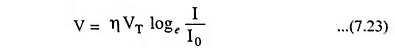
The exponential relationship of the current I to the voltage V holds over many decades of current (a span of as many as seven decades—i.e., a factor of 107—can be found). This is quite a remarkable property of junction diodes, one that is also found in bipolar junction transistors and that has been exploited in many interesting applications.
From Eq. (7.22), the currents I1 and I2 for voltages V1 and V2 are given respectively by equations
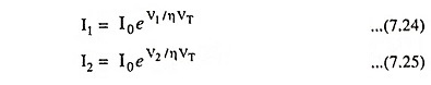
Dividing Eq. (7.25) by Eq. (7.24), we have
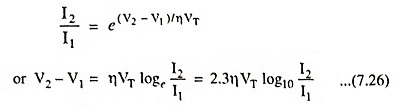
The above equation reveals that for a decade (factor of 10) change in diode current, the diode voltage drop changes by 23ηVT, which is about 60 mV for η = 1 and 120 mV for η = 2. This also suggests that the diode volt-ampere characteristic is most conveniently drawn on semi log paper. Using the vertical, linear axis for V and horizontal, log axis for current I, we have a straight line with a slope of 23ηVT per decade of current. Finally, it is noteworthy that not knowing the exact value of η, circuit designer use the convenient approximate number of 0.1 V/decade for the slope of the diode logarithmic characteristic.
Voltage-current characteristic in the forward region (Fig. 7.15) reveals that the current is negligibly small for voltage smaller than about 0.5 V. This value is usually referred to as the cutin voltage. It needs to be emphasized, however, that this apparent threshold in the characteristic is simply a consequence of the exponential relationship. Another consequence of this exponential relationship is the rapid increase of current I. Thus, for a “fully conducting” diode, the average drop lies in a narrow range, approximately 0.6 V to 0.8 V. This gives rise to a simple “model” for the diode where it is assumed that a conducting diode has approximately 0.7 V drop across the diode. Diodes with different current ratings (i.e., different areas and correspondingly different I0) will exhibit the 0.7 V drop at different currents.
Reverse-Bias Region:
When the diode is reverse biased and V is several times VT in magnitude, current, I = -I0. The reverse current, is, therefore, constant, independent of the applied reverse bias, as shown in Fig. 7.15. Consequently, I0 is referred to as the reverse saturation current.
Real diodes exhibit currents, that though quite small, are much larger than I0. For instance, a small-signal diode whose current I0 is of the order of 10-14 to 10-15 A could show a reverse current of the order of 1 nA. The reverse current also increases somewhat with the increase in magnitude of the reverse voltage. Because of the very small magnitude of the current, these details are not clearly evident on the diode V-I characteristic depicted in Fig. 7.14.
A large component of the reverse current is due to leakage effects. These leakage currents are proportional to junction area, just as I0 is. Their dependence on temperature, however, is different from that of I0. Thus, whereas I0 doubles for every 5°C rise in temperature, the corresponding rule of thumb for the temperature dependence of the reverse current is that it doubles for every 10°C rise in temperature.
Breakdown Region:
The third distinct region of diode operation is the breakdown region, which can be easily identified on the volt-ampere characteristic depicted in Fig. 7.15. The breakdown region is entered when the magnitude of the reverse voltage exceeds a threshold value that is specific to the particular diode, called the breakdown voltage. This is the voltage at the “knee” of the V-I characteristic curve in Fig. 7.15, and is denoted by VZK, where the subscript Z stands for zener and K denotes knee.
As can be seen from Fig. 7.15, in the breakdown region the reverse current increases rapidly, with the associated increase in voltage drop being very small. Diode breakdown is normally not destructive provided that the power dissipated in diode is limited by external circuitry to a “safe” level. This safe value is normally specified on the data sheets of the device. It is, therefore, necessary to limit the reverse current in the breakdown region to a value consistent with the permissible power dissipation.
The fact that the diode V-I characteristic in breakdown region is almost a vertical line enables it to be used in voltage regulation.