Parameters of JFET:
JFET has certain parameters which determine the performance. Such Parameters of JFET are (i) ac drain resistance, (ii) transconductance, (iii) amplification factor, and (iv) dc drain resistance, as explained below:
1. AC Drain Resistance: It is defined as the ratio of change in drain-source voltage to change in drain current at constant gate-source voltage and is denoted by rd.
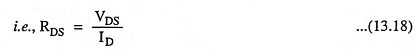
i.e. AC drain resistance,
![]()
It is also called the dynamic drain resistance.
Referring to the output or drain characteristic shown in Fig. 13.8 (b), it is clear that in the active region the change in drain current, ID is very small for change in drain-source voltage, VDS because the characteristic curves are almost flat. Hence ac drain resistance of a JFET is very large ranging from 10 kΩ to 1 MΩ.
2. Transconductance: The control that the gate-source voltage has over the drain current, ID is measured by transconductance. It is denoted by gfs. It may be defined as the ratio of change in drain current to the change in gate-source voltage at constant drain-source voltage.
i.e. Transconductance,
![]()
It is also called the forward transconductance (gfs) or forward transadmittance (Yfs). It is measured in mA/volt or millisiemens.
The transconductance measured at IDSS is denoted by gmo.
Mathematical Expression For Transconductance:
Differentiating both sides of Shockley equation
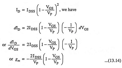
Substituting VGS = 0 in above equation, we get
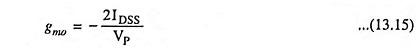
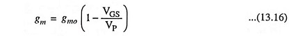
From Eqs. (13.14) and (13.15) we have
3. Amplification Factor: It is defined as the ratio of change in drain-source voltage to the change in gate-source voltage at constant drain current and is denoted by μ.
i.e. Amplification factor,
![]()
Amplification factor of a JFET indicates how much more control the gate-source voltage has over drain current in comparison to the drain-source voltage.
Amplification factor,
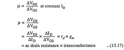
Amplification factor μ of a FET may be as high as 100.
4. DC Drain Resistance: It is also called the static or ohmic resistance of the channel and is defined as ratio of drain-source voltage and drain current. It is denoted by RDS