JFET Bias Circuit Design:
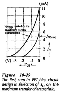
Design Approach – Design of JFET Bias Circuit Design is just as simple as design of BJT bias circuits. One major difference is that FET circuit design normally uses a graphical approach involving the drawing of a bias line on the device transfer characteristics, as in the case of FET circuit analysis. Normally the type number of the FET to be used in the circuit is known, and the maximum and minimum transfer characteristics are available or can be plotted. A maximum drain current (ID(max)) is selected at a point on the maximum transfer characteristic (see Fig. 10-29), and the bias line is drawn through this point. As will be explained, this procedure applies to all types of bias circuits. The selected level of (ID(max)) is used to calculate the values of resistors connected to the drain and source terminals.
Instead of using the maximum transfer characteristics, suppose that the minimum characteristics, or some characteristic between the maximum and minimum, is used in the circuit design. Now, if the FET happens to have the maximum transfer characteristic for the device type number, ID will be larger than the design value. Consequently, the resistor voltage drops (IDRD and IDRS) will be greater than intended (see Fig. 10-30). In this case, VDS will be smaller than its design level, the FET might be forced into the channel ohmic region of its characteristics, and the circuit is unlikely to function correctly. 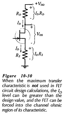
Therefore,
always use the device maximum transfer characteristic when designing a JFET Bias Circuit Design.
As already explained, a FET has a very high input resistance, so high-value bias resistors can be used at the gate terminal. However, there are disadvantages to using extremely high resistance values. A charge accumulated at the gate can take a long time to leak off through a very high resistance. In this case, the gate voltage might not be a stable quantity, and consequently, the drain current could be unpredictable. High-value bias resistors also generate unwanted thermal noise, and they readily pick-up stray radio-frequency signals. For these reasons, 1 MΩ is normally a reasonable upper limit for bias resistors.
In all situations where resistor values are calculated, the closest standard-value components are selected. Normally, ±10% tolerance resistors are always used, and the more expensive ±5% and ±1% components are employed only where greater precision is required.
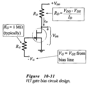
Gate Bias Circuit Design:
Design of a gate bias circuit is very simple. As explained, the desired maximum ID level is marked on the maximum transfer characteristics for the FET. The bias line is drawn vertically through this point, and the required gate bias voltage (-VG) is indicated where the bias line intersects the VGS scale.
![]()
Because the circuit design uses ID(max), the voltage drop across RD is a maximum, and consequently, the drain-source voltage (VDS) is a minimum. So, the drain resistor is calculated as,
As discussed, the bias resistor (RG) is usually selected as 1 MΩ although a lower resistance value may be used. Figure 10-31 shows the equations involved in designing a JFET Bias Circuit Design.
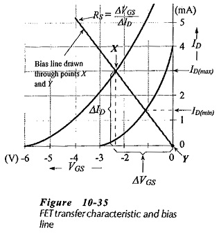
Self Bias Circuit Design:
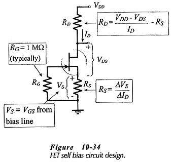
As for gate bias, the procedure for designing a self bias circuit (Fig. 10-34) commences with ID(max) being marked on the FET maximum transfer characteristic (Fig. 10-35). The bias line is then drawn through this point and the point where IDS = 0 and VGS = 0. The value of the source resistor (RS) is determined from the slope of the bias line,
The total resistance in series with the FET drain-source terminals (Fig. 10-34) is (RD + RS). So, Eq. 10-9 can be modified to calculate this quantity,
With RS already known, RD is easily determined. Gate resistor RG is normally selected as 1 MΩ, or lower, as discussed. Figure 10-34 shows the equations for designing a self bias circuit.
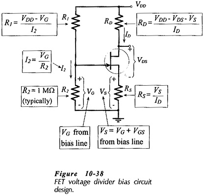
Voltage Divider Bias Circuit Design:
As always, circuit design commences with the specification of VDD, ID(max) and VDS(min). The maximum drain current is plotted on the device maximum transfer characteristic, then either the resistance of RS or the level of VG must be determined before the bias line can be drawn for a voltage divider JFET Bias Circuit Design.
With VDS(min) specified, the remaining portion of the supply voltage (VDD – VDS(min)) is split between VS and VRD. Maximum gain is achieved by selecting RD as large as possible and for a given level of ID this requires the greatest possible voltage VRD. However, the best bias stability is achieved by selecting RS as large as possible, and this indicates maximum VS. A reasonable compromise between these two conflicting requirements (maximum VRD and maximum VS) is to simply make the two voltage drops (and the two resistors) equal. Equation 10-11 is used to calculate (RD + RS), and this is divided to give two equal resistors.
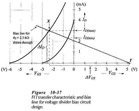
Once RS is determined, the bias line can be drawn through ID(max) with the slope of the line set by RS. This requires that the VGS scale be extended positively, as shown in Fig. 10-37.
From Eq. 10-10,
![]()
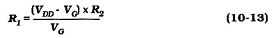
The gate bias voltage (VG) is read from the intersection of the bias line and the (extended) VGS scale (Fig. 10-37). R2 is normally the smallest resistor in the voltage divider. So, R2 is usually selected as 1 MΩ, for the reasons already discussed for RG in the gate bias and self bias circuits. R1 is then calculated from R2 and the resistor voltage drops. From Eq. 10-7,
Another approach that can be used to determine RS is to specify a minimum drain current, and mark ID(min) on the minimum drain characteristic (after marking ID(max)). The bias line is then drawn through the ID(max) and ID(min) points. The slope of the bias line and its intersection with the VGS scale dictates RS and VG, respectively. The design equations for a voltage divider bias circuit are shown on Fig. 10-38.
Designing with Standard-Value Resistors:
Each time a resistor value is calculated the nearest (higher or lower) standard value should be selected, as shown in the preceding examples. Sometimes it will be appropriate to select a resistance higher than the calculated value, and sometimes a lower value should be used. For example, if a resistance is calculated using a minimum current level, it is usually best to select a lower resistance value so that the current is higher than the specified minimum. Regardless of how the standard values are selected, the new current level or voltage drop produced by the standard value component should be calculated before proceeding with the design.