What is Current Mirror? – Circuit Diagram and its Workings
The two-transistor current source, also called a current mirror, is the basic building block in the design of integrated circuit current sources. Figure 20.25 (a) depicts the basic current-source circuit, which consists of two matched or identical transistors Q1 and Q2, operating at the same temperature, with their base terminals and emitter terminals connected together. The base-emitter voltage, VBE is, therefore, the same in the two transistors. Transistor Q1 is connected as a diode; consequently, when the supply voltage is applied, the base-emitter junction of transistor Q1 is forward biased and a reference current IREF is established.
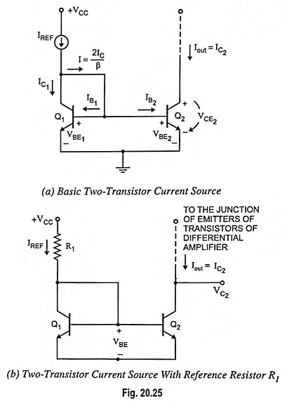
Although there is a specific relationship between IREF and VBE1, VBE1 can be thought of as the result of IREF. Once VBE1 is established, it is applied to the base-emitter junction of transistor Q2. The applied VBE2 turns Q2 on and generates the output current, which is employed to bias a transistor or transistor circuit.
The reference current in the two-transistor current source can be established by connecting a resistor to the supply source +VCC as shown in Fig. 20.25 (b). The reference current is then
![]()
where VBE is the base-emitter voltage corresponding to collector current (IREF).
Connecting the base and collector terminals of a BJT effectively provides a two-terminal device with ampere-volt characteristics that are identical to the iC versus vBE characteristic of the BJT.
Current Relationships: Figure 20.25 (a) depicts the current in the two-transistor current source. Since VBE is the same in both devices, and the transistors are identical, then IB1 = IB2 and IC1 = IC2. Transistor Q2 is assumed to be biased in the forward-active region. Applying Kirchhoff’s current law to the collector node of transistor Q1, we have
![]()
Replacing IC1 by IC2 (i.e., IC1 = IC2) and noting that IB2 = IC2/β, above equation becomes

i.e., the constant current provided at the collector of transistor Q2 mirrors that of transistor Q1
Since

The current IREF set by VCC and R1 is mirrored in the current into the collector of transistor Q2.
Transistor Q1 is referred to as a diode-connected transistor because its base and collector are shorted together.
The operation of the current mirror may be described as follows:
- Q1 acts like a diode and a current is established through it.
- Q1 will develop a voltage drop VBE, in response to the current.
- The base-emitter of Q2 is in parallel with that of Q1 (VBE1 = VBE2 = VBE).
- Q2‘s collector current will be established in response to its VBE.
- Since the two transistors are matched, Q2‘s collector current will be approximately equal to Q1‘s collector current. Q2‘s collector current is said to “mirror” the current through Q1.
Q1 is often called a compensating diode because it automatically compensates for variations in temperature. Matching of diode curve means matching at all temperatures as well as voltages. When the temperature increases, the voltage across the emitter diode falls approximately 2 mV per degree. Since the voltage across the compensating diode also decreases by 2 mV per degree, the collector current is little affected with temperature increase.
Modified Current Mirror:
Equation (20.48) reveals that the collector current in the transistor Q2 is related to the reference current IREF by a factor (β+2/β). For β >> 2, IC2 = IREF1, but for low-current transistors IC2 can differ significantly from IREF. However, this error can be reduced by introducing another transistor as an emitter follower. The resulting circuit, as shown in Fig. 20.26, is a modified current mirror circuit or three-transistor current source. We again assume that all transistors are identical; therefore, since the VBE is the same for transistors Q1 and Q2, IB1 = IB2 and IC1 = IC2. Transistor Q3 supplies the base currents to Q1 and Q2, so these base currents should be less dependent on the reference current. Also, since the current in transistor Q3 is substantially smaller than that in either Q1 or Q2, the current gain of Q3 is expected to be less than those of transistors Q1 and Q2. We may define the current gains of transistors Q1 and Q2 as β1 = β2 = β, and current gain of the transistor Q3 as β3.
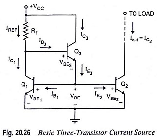
Applying Kirchhoff’s current law to the collector node of transistor Q1, we have
Combining above Eqs. (20.49), (20.50) and (20.51), we have

Replacing IC1 by IC2 and noting that IB2 = IC2/β, the above Eq. (20.52) may be rewritten as

The output or bias current is then

The reference current is given by

As a first approximation base-emitter voltages of transistors Q1 and Q3 are assumed to be equal (i.e. VBE3 = VBE1) as indicated in Eq. (20.55).
A comparison of Eq. (20.54) for the three-transistor current source and Eq. (20.48) for the two-transistor current source reveals that the approximation of Iout ≡ IREF is better for three-transistor circuit.
Note : For a two-transistor current source (Fig. 20.25) and for a three-transistor current source (Fig. 20.26), a large valued resistor R1 is required for a small biasing current, which is not feasible because it becomes costly in terms of chip area. Usually, these current sources are employed for producing a current of about 0.3 mA-0.5 mA.
Multiple Current Source:
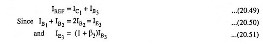
In the previous current sources, we established a reference current IREF and one load current Iout. In the two-transistor current source in Fig. 20.25 (a), the base-emitter junction of the diode-connected transistor Q1 is forward biased, when the bias voltage +VCC is applied. Once VBE is established, the voltage is applied to the base-emitter junction of transistor Q2, which turns Q2 on and generates the output current Iout. The base-emitter voltage of transistor Q1 can also be applied to additional transistors, to generate multiple load currents. Consider the circuit shown in Fig. 20.27. Transistor QR, which is the reference transistor, is connected as a diode. The resulting base-emitter voltage of reference transistor QR, established by reference current IREF, is applied to N output transistors, producing N load currents.
The relationship between each load current and the reference current, assuming all transistors are matched, is

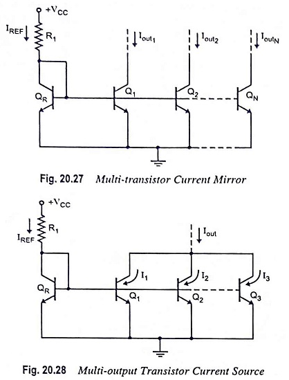
The collectors of multiple output transistors can be connected together, changing the load current versus reference current relationship. For an example, the circuit depicted in Fig. 20.28 has three output transistors with common collectors and a load current Iout. Assuming that transistors QR, Q1, Q2 and Q3 are all matched if the current gain β is very large, the base currents can be neglected and I1 = I2 = I3 = IREF, and the output current lout = 3IREF. This process is not recommended for discrete devices, since a mismatch between devices will usually cause one device to carry more current than the other devices. Connecting transistors in parallel increases the effective base-emitter area of the device. In actual IC fabrication, the base-emitter area would be doubled or tripled to provide an output current twice or three times the value of IREF.
Wilson Current Source:
This is another configuration of a three-transistor current source, known as a Wilson current source. The circuit is shown in Fig. 20.29. This circuit has a large output resistance. We again assume that all the transistors are identical, with IB1 = IB2 = IB; IC1 = IC2 and VBE1 = VBE2.
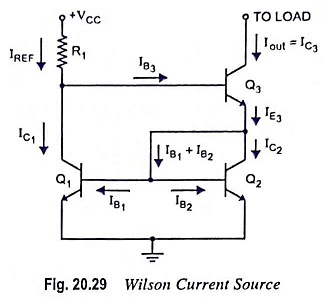
Applying KCL at the emitter of transistor Q3, we have
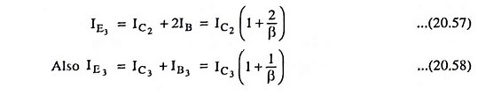
Comparing Eqs. (20.57) and (20.58), we have
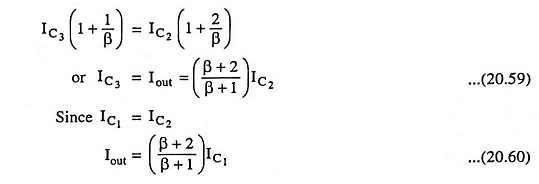
Applying KCL at the collector of transistor Q1
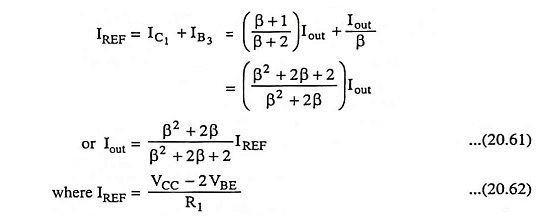
The difference

is extremely small error for modest values of β.
In the Wilson current source, the output resistance looking into the collector of Q3 is Rout ≡ βr03/2, which is approximately a factor β/2 larger than that of either the two-transistor source or the basic three-transistor source. This means that, in the Wilson current source the change in bias current Iout with a change in output collector voltage is much smaller.
Widlar Current Source:
The basic current mirror shown in Fig. 20.25 (b) has a limitation that for low value current source the resistance R1 required is sufficiently large and cannot be fabricated economically in IC circuit. For a two-transistor current shown in Fig. 20.25 (b), if a load current of Iout = 10μA is required, then for VCC = 10 V, the required resistance value is

The solution to above problem is a circuit shown in Fig. 20.30, called a Widlar current source. This circuit is particularly suitable for low value of current. The circuit differs from the basic current mirror [Fig. 20.25 (b)] only in the resistance RE that is included in the emitter lead of transistor Q2. A voltage difference is caused across emitter resistor RE1 so that the VBE2 is lesser than VBE1. A smaller VBE produces a smaller collector current. It means that the load current Iout is lesser than reference current IREF.
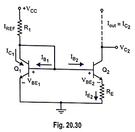
For β >> 1 for transistors Q1 and Q2 and for transistors to be identical
Subtracting Eq. (20.67) from Eq. (20.66), we have
From the circuit, we see that

Comparing Eqs. (20.68) and (20.69), we have
Equation (20.70) provides the relationship between the reference and bias currents. Sometimes, emitter resistances are used in both the transistors Q1 and Q2 as depicted in Fig. 20.31.
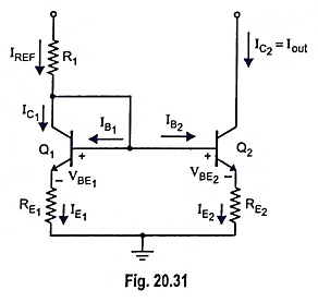
From the circuit shown in Fig. 20.31.
Applying KVL in the base-emitter loop, we have
Comparing Eqs. (20.72) and (20.73), we have
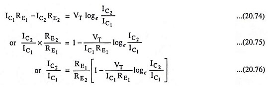
For the range 0.1 < IC2/IC1 < 10 it can be assumed that IC2/IC1 ≡ RE1/RE2. Thus even large ratio is obtained by the modified circuit (Fig. 20.31).