Generation of DSBSC Signal using Balanced and Ring Modulator:
DSBSC signal can be obtained by simply multiplying the modulating signal with the carrier signal. By simple multiplication of Vc sin ωct and Vm sin ωmt, we have the lower and upper sidebands without carrier as shown below:
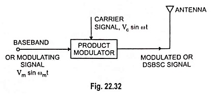
It means that a DSBSC signal is obtained by simply multiplying modulating signal (Vm sin ωmt) with carrier signal (Vc sin ωct). This is achieved by a product modulator. The block diagram of a product modulator is depicted in Fig. 22.32.
Here we will discuss two types of product modulators namely the balanced modulator and ring modulator.
Balanced Modulator:
We know that a nonlinear resistance or a nonlinear device may be used to provide amplitude modulation, i.e., one carrier and two sidebands. However, a DSBSC signal contains only two sidebands. Thus, if two nonlinear devices such as diodes, transistors etc. are connected in a balanced mode so as to suppress the carriers of each other, then only sidebands are left, i.e., a DSBSC signal is produced. Thus, a balanced modulator may be defined as a circuit in which two nonlinear devices are connected in a balanced mode to generate a DSBSC signal.
Two balanced modulator circuits using diodes and transistors as nonlinear devices are shown in Figs. 22.33 (a) and 22.33 (b).
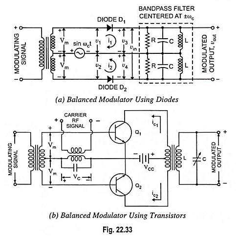
It is assumed that both diodes and transistors used in circuits shown in Fig. 22.33 have identical characteristics and that the circuit is symmetrical with respect to the centre tap of the transformer. As the two halves have to be matched or balanced, such a modulator is known as a balanced modulator.
The modulating signal Vm sin ωmt is applied in push-pull and the carrier RF signal Vc sin ωct is put in parallel to a pair of identical diodes D1 and D2 [Fig. 22.33 (a)] or two matched transistors Q1 and Q2 [Fig. 22.33 (b)]. In transistor circuit the carrier RF signal is thus applied to the bases of the two transistors in phase, while the modulating signal appears 180° out of phase at the bases, as they are at the opposite ends of a centre-tapped transformer.
A bandpass filter used in diode circuit [Fig. 22.33 (a)] is that of type filter which allows to pass a particular hand of frequencies only. Here since the bandpass filter is centred around ±ωc, it will pass a narrowband of frequencies centred at ±ωc with a small bandwidth of 2ωm to preserve the sidebands.
The modulated output currents of the two transistors Q1 and Q2 are combined in the centre-tapped primary of the push-pull output transformer. These currents, therefore, are opposite and subtract as indicated by the direction of arrows in the figure. For a symmetrical arrangement, the carrier frequency will be completely cancelled.
It may be proved that the output signal (or modulated signal) contains only sidebands with carrier component completely eliminated as below.
The expression for the modulated wave generated by transistor Q1 may be given as

The modulated wave generated by transistor Q2 will be the same as the generated by Q1 except that it will have a phase difference of 180° (i.e., reversed phase). So
![]()
At the output transformer, the output voltage vout, due to push-pull arrangement, is proportional to (v1 – v2), so
Modulated output,
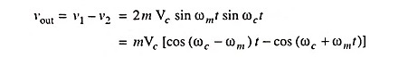
Thus, it is proved that the output signal consists of only sidebands and the carrier component is eliminated.
Ring Modulator:
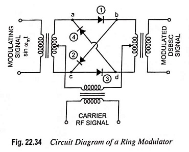
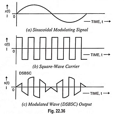
Ring modulator is another product modulator, which is used to generate DSBSC signal. Figure 22.34 shows the circuit diagram of a ring modulator. In a ring modulator circuit, four diodes are connected in the form of a ring in which all four diodes point in the same manner. All the four diodes in ring are controlled by a square wave carrier signal of frequency ωc applied through a centre-tapped transformer. If the diodes are ideal and the transformer is perfectly balanced, the outer diodes are switched on if the carrier signal is positive whereas the two inner diodes are switched off and thus presenting very high impedance as shown in Fig. 22.35 (a). Under this condition, the modulator multiplies the modulating signal by +1. Now, in case when carrier signal is negative, the situation becomes reversed as depicted in Fig. 22.35 (b). In this case modulator multiplies the modulating signal by -1. Thus, the ring modulator is a product modulator for a square wave carrier and modulating signal.
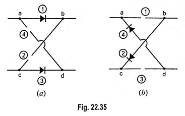
Figure 22.36 illustrates the modulating signal (assuming a sinusoidal signal), square-wave carrier signal and modulated (DSBSC) signal.