What is MOS Capacitor?
The metal-oxide-semiconductor MOS capacitor shown in Fig. 13.92 (a) is the heart of the MOSFET. The metal may be aluminium or some other type of metal. In most cases, the metal is replaced by a high-conductivity polycrystalline silicon layer deposited on the oxide. However, the term metal is still used in referring to MOSFETs. In the figure, the parameter tox is the thickness of the oxide and εox is the permittivity of the oxide.
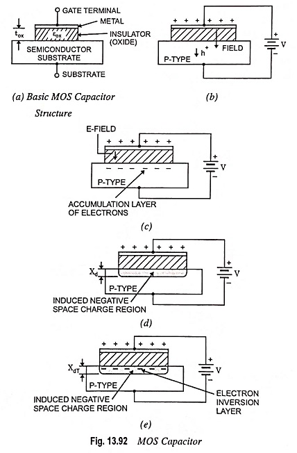
A MOS capacitor with a P-type semiconductor substrate is shown in Fig. 13.92 (b). The top metal terminal, also known as the gate, is at a positive voltage with respect to the semiconductor substrate. We can see that a positive charge will exist on the top metal plate and an electric field will be induced in the direction shown in the figure. If the electric field penetrates the semiconductor, holes in the P-type material will experience a force away from the oxide-semiconductor interface. As the holes are pushed away from the interface, a negative space-charge region is produced, because of the fixed capacitor impurity atoms. The negative charge in the induced depletion region corresponds to the negative charge on the bottom plate of the MOS capacitor. Figure 13.92 (d) shows the equilibrium distribution of charge in the MOS capacitor with this applied voltage.
When a larger positive voltage is applied to the gate, the magnitude of the induced electric field increases. Minority carrier electrons are attracted to the oxide-semiconductor interface as shown in Fig. 13.92 (e). This region of minority carrier electrons is known as an electron inversion layer. The magnitude of the charge in the inversion layer is a function of the applied gate voltage.
The same basic charge distribution can be obtained in a MOS capacitor with an N-type substrate.
The term enhancement mode means that a voltage must be applied to the gate to produce the electron inversion layer. For the metal-oxide-semiconductor capacitor with a P-type substrate, a positive voltage must be applied to produce the electron in version layer, for the MOS capacitor with an N-type substrate, a negative gate voltage must be applied to produce the hole inversion layer.