Capacitor Coupled Common Base Amplifier:
A practical Capacitor Coupled Common Base Amplifier (using a plus/minus supply) is shown in Fig. 12-39. [Note the polarity of the input coupling capacitor (C1).] The CB circuit is analysed already, where it is found to have a very low input impedance, as well as a voltage gain and output impedance similar to a CE circuit, Because the CB circuit has no phase inversion between the input and output terminals, there is no Miller-effect amplification of the collector-base capacitance. Consequently, a CB circuit is capable of operating at much higher frequencies than a CE circuit.
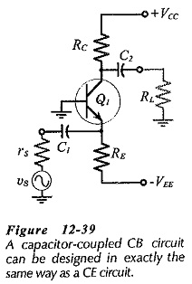
Design procedure for a CB circuit is exactly the same as that for a CE circuit. Resistor calculation is performed just as if a CE circuit were being designed. The output coupling capacitor (C2 in Fig. 12-39) is determined in the usual way. Because of the very low input impedance of a CB circuit, the input coupling capacitor (C1) is the largest capacitor in the circuit. So, C1 determines the circuit low cutoff frequency, and its capacitance is calculated like an emitter bypass capacitor in a CE circuit.
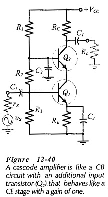
Cascode Amplifier:
The very low input impedance of a CB circuit (typically 25 Ω) is a major disadvantage. To increase the circuit input impedance while retaining its high frequency performance, the cascode amplifier (Fig. 12-40) uses a CE input stage driving a CB output stage Transistor Q1 and its associated components operates as a CE input stage, while the circuit of Q2 functions as a CB output stage.
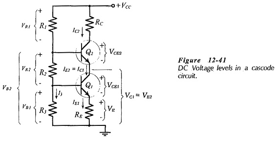
The circuit dc voltage and current levels are illustrated in Fig. 12-41. It is seen that IE1 is set by VB1 and RE. Collector current IC1 approximately equals IE1 and IE2 is the same current as IC1. So, IC2 approximately equals IE1. The current levels remain constant so long as ICE1 and ICE2 are large enough for transistor operation.
A positive-going ac signal at the base of Q1 produces an increase in IE1 and this results in an IC2 increase. Thus, the voltage drop across RC is increased, producing a decrease in the output voltage. So, there is an ac phase inversion between the input and output.
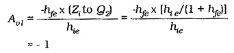
The input impedance at the emitter of Q2 constitutes the load for the collector of Q1. Therefore, the voltage gain from the circuit input to Q1 collector is,
With an input stage gain of -1, there is no significant Miller effect at the circuit input.
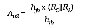
The voltage gain produced by the Q2 CB circuit is,
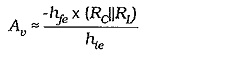
Converting to CE parameters, the overall voltage gain for the cascode amplifier is the same as that for a CE circuit;
Design Calculations:
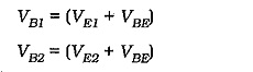
The design procedure for a cascode amplifier is easily derived from the CE design process. The voltage across RE should typically be 5 V, and the VCE for each transistor should be a minimum of 3 V. The emitter voltage for Q2 is,![]()
The transistor base voltages are,
When the voltage and current levels are selected, the resistor values are easily calculated.
The base bypass capacitor (C2) in Fig. 12-40 should have an impedance equal to one tenth of the hie of Q2. This ensures that the impedance looking into Q2 emitter terminal is not significantly affected by R1 and R2. Also, that no portion of the input signal (at Q2 base) is developed at Q1 base.
Differential Amplifier as a High-Frequency Amplifier:
The differential amplifier discussed already can have the same high-frequency performance as a CB circuit. The differential amplifier circuit shown in Fig. 12-43, has zero voltage gain from Q1 base to Q1 collector, because there is no collector resistor. Consequently, there is no Miller effect on the input capacitance.
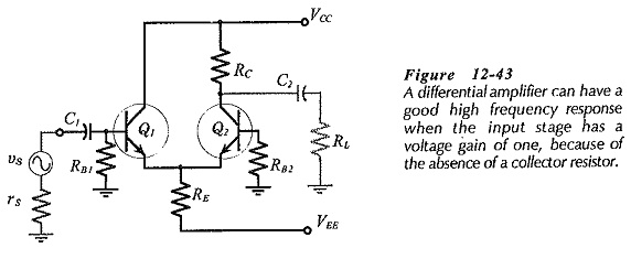
Also, the amplifier input is applied (via Q1) to the emitter of Q2, as in the case of a CB circuit. So, there is no Miller effect associated with Q2. The input impedance (at the base of Q1) is reasonably high, like a CE circuit and unlike the case of a Capacitor Coupled Common Base Amplifier.