Capacitor Coupled Two Stage CE Amplifier:
A Capacitor Coupled Two Stage CE Amplifier circuit is shown in Fig. 12- 15 .
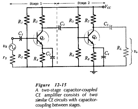
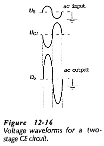
Stage-1 is capacitor-coupled (via C3) to the input of Stage-2. The signal is applied to the input of Stage-1, and the load is coupled to the output of Stage-2. The signal is amplified by Stage-1, and the output of Stage-1 is amplified by Stage-2, so that the overall voltage gain is much greater than the gain of a single stage. As illustrated by the circuit waveforms in Fig. 12-16, the signal voltage is phase-shifted through 180° by Stage-1, and through a further 180° by Stage-2. Consequently, the overall phase shift from input to output is zero (or 360°).
Circuit Design:
The simplest approach to design of this circuit is to make each stage identical. Then, when Stage-2 has been designed, the components for Stage-1 are selected as: R1 = R5, R2 = R6, R3 = R7, R4 = R8, C1 = C3, and C2 = C4. Note that C3 is calculated in terms of the input resistance to Stage-2, which should be identical to that for Stage-1 if the stages are otherwise identical. C5 is calculated in the usual way for an output coupling capacitor.
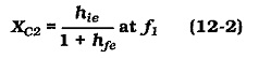
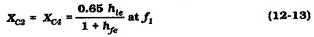
One way the design of a two-stage circuit differs from that of a single-stage circuit is in determination of emitter bypass capacitors C2 and C4. Consider Eq. 12-2, which was derived to calculate a bypass capacitor value to make the voltage gain of a single-stage circuit 3 dB down from the mid-frequency gain at the selected lower cutoff frequency (f1).
If this equation is used to calculate the capacitance of C2 and C4 in the two-stage circuit, it is found that the gain of Stage 1 is down by 3 dB at f1, and the gain of Stage 2 is also down by 3 dB at f1, (see Fig. 12-17).
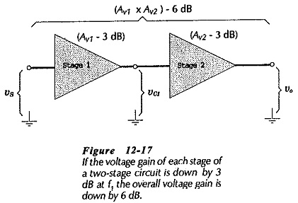
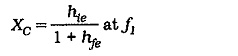
This means that the overall gain of the circuit is down by a total of 6 dB at frequency f1. For a 3 dB decrease in overall voltage gain at f1, the bypass capacitors must be calculated to give a 1.5 dB reduction in the gain of each stage. A 1.5 dB reduction in stage gain at f1, is achieved by making the reactance of the emitter bypass capacitor equal to 0.65 limes the impedance in series with the capacitor. Thus, the equation for the bypass capacitor impedance now becomes,
Circuit Analysis:
Ac analysis of a two-stage, Capacitor Coupled Two Stage CE Amplifier is similar to analysis of single-stage circuits, as already discussed. The h-parameter equivalent circuit for the amplifier circuit in Fig. 12-15 is drawn in Fig. 12-19. Once again, this equivalent circuit is produced by replacing the supply voltage and all capacitors with short circuits, and substituting device h-parameter models for each, transistor. The resultant equivalent circuit simply consists of two single-stage h-parameter equivalent circuits. As always, voltage polarities and current directions are indicated for an instantaneous positive-going signal voltage. The voltage polarities show a 180° phase shift between vi and vc1, and a further 180° phase shift between vc1, and vo.
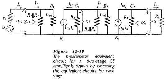
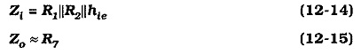
The performance equations for the two-stage circuit are readily derived from the equations for a single-stage circuit. Input and output impedance are exactly the same as for the single-stage circuit:
The voltage gain equation for the second stage is exactly the same as the single-stage gain equation. The Capacitor Coupled Two Stage CE Amplifier load at the collector terminal of the first stage is the input impedance of the second stage So the voltage gain equations are,
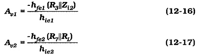
The overall voltage gain is found by multiplying the two individual stage gains:
![]()
Equations for current gain and power gain can also be derived from the single-stage equations, but these quantities are normally not important.