Two Stage Direct Coupled Common Emitter Amplifier:
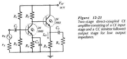
Figure 12-23 shows Two Stage Direct Coupled Common Emitter Amplifier. This time the second stage is a common collector circuit, or emitter follower. Stage 2 gives the circuit a very low output impedance, but has unity voltage gain Stage 1 still has substantial voltage gain.
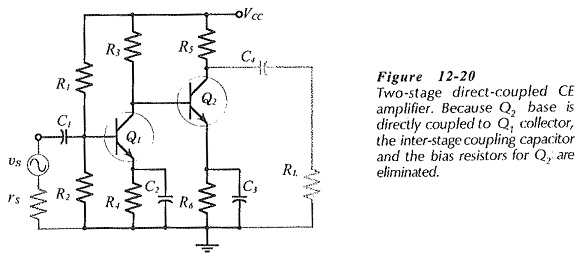
The design procedure for this circuit is similar to the procedures already discussed. As with the circuit in Fig. 12-20, the Q2 base bias voltage is the collector voltage of Q1. A suitable level of emitter current IE2 is selected, and RE is calculated to be (VB2 – VBE)/IE2. Coupling capacitor C1 is once again calculated from XC1 = Zi/10.
The load resistor (RL) may be relatively small, which means that coupling capacitor C3 must be large. Therefore, both C2 and C3 are used to determine the low 3 dB frequency of the circuit by using the 0.65 factor employed in Eq. 12-14.
It is important to realize that the emitter follower in Fig. 12-23 is a small-signal circuit. In fact, this type of circuit functions best when the amplitude of the at output voltage is much smaller than the dc base-emitter voltage of the output transistor (VBE). With at output voltages that approach or exceed VB2, the base-emitter junction of Q2 might become reverse biased when the output voltage moves rapidly in a negative direction. In this case, the circuit will not function correctly. Where large output voltages and low output impedance are required, a complementary emitter follower is used.
With the second stage operating as a small-signal emitter follower, resistor R5 in Fig. 12-23 does not have to be very much smaller than external load RL. However, for satisfactory operation, Q2 emitter current (IE2) should be greater than the peak ac load current (ip). The peak output current is calculated by dividing the desired peak output voltage vp, by the load resistance; ip = vp/RL.

