Compensating Network in Op Amp:
In op-amps the variations in gain and phase shift with respect to frequency are due to the internal capacitors and stray capacitances, which are due to physical characteristics of semiconductor devices (BJTs and FETs) and the internal construction of the op-amp. The rate of change of gain as well as the phase shift of an op-amp can be controlled by adding specific components, most common of which are resistors and capacitors. The network formed by such components and employed for modifying the rate of change of gain and phase shift is known as compensating network. The main purpose of a Compensating Network in Op Amp is to improve the performance of an op-amp circuit over the desired frequency range by controlling its gain and phase shift.
First generation op-amps such as 301, 709 have no internal frequency compensation, whereas later-generation op-amps such as 741, 351 and 318 have internal compensation. Thus op-amps are of two types viz. internally compensated and externally compensated.
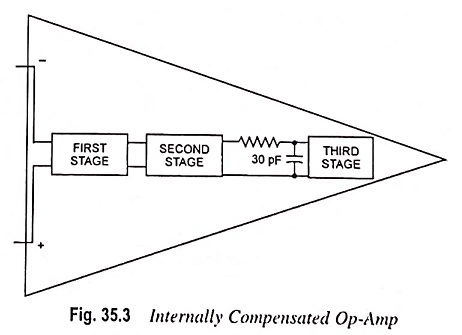
The internally Compensating Network in Op Amp use a metal oxide capacitor built within the IC. The circuit configuration is given in Fig. 35.3. Although this works well, internal compensation does not allow us any control over the op-amp frequency response.
The 301 and 709 op-amps have no internal frequency compensation capacitor. Instead, frequency compensation terminals are provided, and compensation capacitors are to be connected externally. Failure to connect these external compensation capacitors will practically guarantee that the op-amp will oscillate. However, the op-amp’s frequency response can be tailored as per needs by the value and type of compensation network used.
The Compensating Network in Op Amp for modifying the rate of change of gain and the phase shift are of two types viz. the phase lag and phase lead. These two networks are indicative of their functions, since phase lag contributes a negative phase angle and phase lead a positive phase angle. In each case an R – C network is connected into the circuit to form as a part of loop. Usually, as recommended by the device manufacturer, the R – C network is connected to specified points within the op-amp. For this purpose, external terminals are provided for access to points inside the IC.
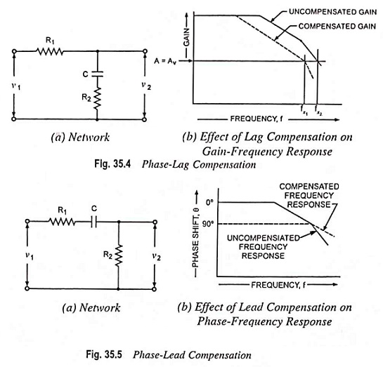
A phase-lag network stabilizes an amplifier by reducing the open-loop gain, so that the frequency at which Aβ = 1 occurs when the phase shift is too small for instability. The components of the phase-lag network are calculated to introduce additional phase lag at some low frequency where op-amp phase shift θ is still so small that additional shift has no effect. For the circuit shown in Fig. 35.4 (a), it is obvious that at frequencies for XC ≫ R2, the voltage v2 lags behind v1. A phase lag as great as – 90° might be introduced. However, at higher frequencies where XC ≪ R2, no significant phase lag occurs, and the network merely introduces some attenuation. The effect of this attenuation is to move the frequency fx1 at which β A = 1 (for a given closed-loop gain Av) to a lower frequency fx2, as illustrated in Fig. 35.4 (b). Because fx2 is smaller than fx1 the phase shift at fx2 is smaller than that at fx1, and the circuit is likely to be stable.
A phase-lead network cancels some of the phase lag. In the phase-lead network shown in Fig. 35.5 (a) when XC ≫ R1, v2 leads v1. This phase-lead cancels some of the unwanted phase lag in the op-amp, as illustrated in Fig. 35.5 (b), thus making the circuit more stable.
Calculation of component values for an op-amp compensation network may be a tedious job, and the frequency response plot is required for the particular op-amp used. For simplifying the compensation work, IC manufacturers publish recommended compensation networks and the component values on op-amp data sheets. The recommended component values for the amplifier closed-loop gain are noted from the data sheet and then connected to the op-amp, as illustrated on the data sheet.
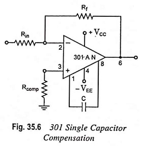
Single capacitor compensation is the simplest compensation and is shown in Fig. 35.6. The minimum value of compensation capacitance is dependent on the resistor feedback network.
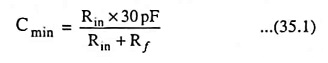
The noteworthy point is that the same equation holds good for inverting as well as noninverting op-amps, so use of noninverting amplifier will allow you to have lower values of Rin and C without sacrificing the input impedance.
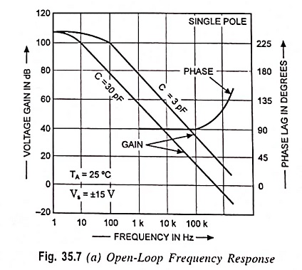
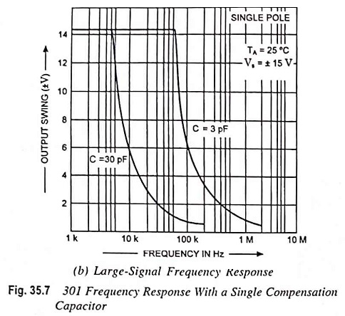
The effects of a 3 pF and a 30 pF compensation capacitor on open-loop frequency response, and output voltage swing are shown in Fig. 35.7. Larger compensation capacitance can be used to lower the frequency response and output voltage swing further.