Transformer Coupled Class A Power Amplifier:
Transformer Coupled Class A Power Amplifier also sometimes referred to as single ended power amplifier. The term “single ended” (denoting only one transistor) is used to distinguish it from the push-pull amplifier using two transistors. In case of a direct coupled class A power amplifier, the quiescent current flows through the collector resistive load and causes large wastage of dc power in it. This dc power dissipated in the load resistor does not contribute to the useful ac output power. Furthermore, it is generally inadvisable to pass the dc through the output device such as in a voice coil of a loudspeaker. For these reasons an arrangement using a suitable transformer for coupling the load (say, a loudspeaker) to the amplifier is usually employed, as shown in Fig. 17.11. This Transformer Coupled Class A Power Amplifier arrangement enhances the conversion efficiency by a factor of 2 by eliminating the dc power dissipation in the load. Since the primary of the transformer has negligible dc resistance, there is negligible dc power lost at this point. The ac power is, however, coupled magnetically across the transformer into the load RL. This Transformer Coupled Class A Power Amplifier method also prevents a large dc current from flowing through the load, which otherwise could be harmful if the load were a loudspeaker, since it would cause saturation of the magnetic circuit and impair the reproduction of the audio signal.
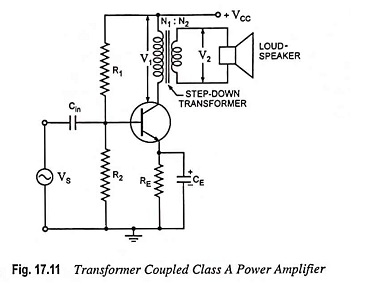
This arrangement also permits impedance matching.
In a power amplifier circuit shown in Fig. 17.11, R1 and R2 provide potential divider biasing and emitter resistor RE is meant for bias stabilization. The emitter bypass capacitor CE is meant for preventing negative feedback in the emitter circuit. The input capacitor Cin couples ac signal voltage to the base of the transistor but blocks any dc from the previous stage. A step-down transformer of suitable turn ratio (a = N1/N2) is provided to couple the high impedance collector circuit to low impedance load.
Impedance Matching:
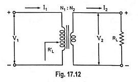
The power transferred from the power amplifier to the load (say a loudspeaker) will be maximum only if the amplifier output impedance equals the load impedance RL. This is in accordance with the maximum power transfer theorem. If we were not able to achieve the above condition, lesser power will be transferred to the load RL, though the amplifier is capable of delivering more power, and rest of power developed would be lost in the active device. Hence for transfer of maximum power from amplifier to the output device matching of amplifier output impedance with the impedance of output device is necessary. This is accomplished by using a step-down transformer of suitable turn ratio. The transformer impedance matching circuit is shown separately in Fig. 17.12, where R′L is the resistance looking into the primary of the transformer and is given as
![]()
Thus the ratio of the transformer input and output resistances varies directly as the square of the transformer turn ratio :
![]()
where a is ratio of primary to secondary turns of step-down transformer, RL is the resistance of load connected across the transformer secondary and R′L is effective resistance looking into the transformer primary.
Circuit Operation of Transformer Coupled Class A Power Amplifier:
In this circuit dc (winding) resistance determines the dc load line. Typically, this resistance is quite small (assumed to be zero) providing dc load to be a vertical line rising from VCC, as shown in Fig. 17.13. When an ac signal is applied to the base of the transistor the collector current will vary around the operating point Q.
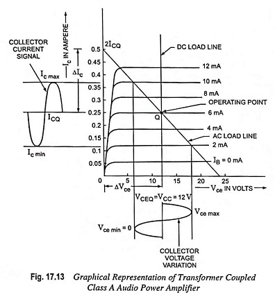
In order to have maximum ac power output, the peak value of collector current due to input ac signal alone should be equal to the zero signal collector current. To achieve this, the operating point Q is located at the centre of the load line. This is achieved by adjusting the biasing circuit (R1, R2 and RE).
When ac signal is applied, collector current fluctuates from maximum to minimum (zero), and operating point Q moves up and down the load line. At the peak of the positive half cycle of the input signal, the total collector current Ic max = 2 ICQ and collector-emitter voltage Vce min = 0 while at the peak of the negative half cycle of the input signal, the collector current Ic min = 0 and collector-emitter voltage Vce max = 2 VCC. Thus collector-emitter voltage varies in opposite phase to the collector current. The variation of collector voltage appears across primary of the transformer. Now ac voltage is induced in the transformer secondary which in turn develops ac power and supplies to the load.
Circuit Analysis:
In an ideal transformer, there is no voltage drop in primary so VCEQ = VCC and power input to the transistor becomes equal to the dc power drawn from the collector supply VCC as power lost in the primary is negligibly small.
Thus power input to the transistor,
![]()
and overall efficiency becomes equal to collector efficiency and
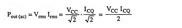
![]()
Under condition of development of maximum ac power, voltage swings from Vce max to zero and collector current from Ic max to zero. So
![]()
AC power developed across the load,
Collector efficiency,
![]()
Thus for a transformer coupled class A power amplifier the maximum theoretical efficiency is 50%. In practice, the efficiency of such an amplifier is somewhat less than 50%. It is about 30%.
The efficiency of a transformer coupled class A power amplifier can be given as
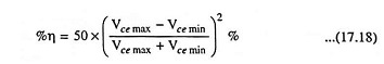
The larger the value of Vce max and smaller the value of Vce min the closer the efficiency approaches the theoretical limit of 50%. Well-designed circuits can approach the limit of 50%. The larger the amount of power handled by the amplifier, the more critical the efficiency becomes. For a few watts of power a simpler, cheaper circuit with less than maximum efficiency is acceptable (and sometimes desirable). For power levels in the tens to hundreds of watts efficiency as close as possible to the theoretical maximum would be desired.
The maximum power dissipated in the transistor is under zero signal condition i.e., VCC ICQ where ICQ is the collector current under zero signal condition.
Since collector current flows at all times throughout the whole cycle, no part of the signal is cut off and thus the output waveform obtained in this case is exact replica of the input waveform. Thus such amplifiers have least distortion. However, they suffer from the drawbacks of (i) low output power and (ii) low collector efficiency (less than 50%; about 30%).
Thus, for a given transistor dissipation capability, the output ac power obtainable in a load is the same (i.e., ideally one half of the amount of power input to the transistor) no matter whether the load is direct coupled or transformer coupled. However, the drain on the power supply in a transformer coupled amplifier is ideally one half of what it is in the direct coupled amplifier.
Collector Dissipation Curve:
In a power amplifier, the main source of power supply is collector dc supply and some of it is converted into ac power and appears in the load and rest of it is dissipated in the form of heat. Thus in a power amplifier
![]()
or Power dissipation,
![]()
From above Eq. (17.19) it is obvious that power dissipated by the transistor (Pd) is the difference of average dc power input from the collector supply battery, Pin (dc) (which is constant for a given battery and operating point) and ac output power, Pout (ac) supplied to the load. For zero output (i.e., when no signal is applied), the transistor is required to dissipate the maximum power i.e., Pd = VCC ICQ. This is the worst case for a transistor. When the signal is applied, the transistor has to dissipate less power. Hence in designing a power amplifier, the important factor that is to be kept in mind is the power dissipation rating of the transistor.
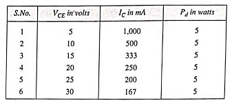
Let the power dissipation capacity of a transistor be 5 W. For designing a power amplifier, first of all its collector dissipation curve is plotted. For plotting the collector dissipation curve of a power amplifier collector current lC is determined corresponding to some arbitrary values of collector-emitter voltage VCE from the relation Pd = VCE IC = 5 W, the power dissipation capacity of the transistor. Some sample calculations are given below in tabular form. The curve obtained from these values is a hyperbola, as shown in Fig. 17.14.
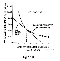
For using this transistor in a power amplifier, its operating point must be below the dissipation curve, otherwise transistor will get damaged. This is the importance of dissipation curve.
Drawbacks of Single Ended Transformer Coupled Amplifier:
A single ended transformer coupled amplifier has the following drawbacks:
- The total harmonic distortion is unacceptably high for most audio applications except in cheaper amplifiers. The second harmonic distortion is usually the greatest offender.
- Maximum output power is delivered at a load resistance that is different from the value for minimum harmonic distortion. Consequently, the amplifier is designed to operate into a load that provides slightly less than maximum output power, but a significantly lower total distortion.
- The output transformer is subject to saturation problems due to flow of direct current in transformer primary.
Output Transformer Saturation:
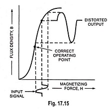
For the proper operation of a transformer, the necessary requirement is that the flux in the transformer core varies in proportion with the variation in primary current. The transformer core is said to be saturated if the core flux does not change in proportion with the change in primary current. The effects of transformer core saturation are as follows:
- With the increase in primary current of transformer, it is possible that there may not be a correct corresponding increase in magnetic flux to induce the proper voltage in the secondary.
- The primary current may increase to a very high value due to sudden reduction in the primary impedance because the saturation of the core will reduce the primary inductance to a very low value.
In a single ended transformer coupled amplifier, the relatively large dc collector current flowing under zero signal condition may cause a large magnetic flux density in the transformer core, that may result in saturation of transformer core. Then, when the collector current increases due to increase in input signal, it is possible that magnetic flux may not increase in proportion to the collector current and so proper voltage may not be induced in the secondary. On the negative swing, however, the collector current would be able to fall and reduce the flux by the correct amount, inducing in the secondary a voltage larger than was obtained on the positive half-cycle, as shown in Fig. 17.15. Thus saturation of output transformer core may result in distorted output.