RC Coupled Transistor Amplifier – Operations, Derivation and Applications:
A two-stage RC Coupled Transistor Amplifier using N-P-N transistors in CE configuration is shown in Fig. 16.12. The two transistors used are identical and use a common power supply VCC. The resistors R1, R2 and RE form the biasing and stabilization network. In this arrangement, the signal developed across collector resistor RC of the first stage is coupled to the base of the second stage through the coupling capacitor CC. As the coupling from one stage to the next is obtained by a coupling capacitor followed by a connection to a shunt resistor, therefore, such amplifiers are called Resistance-capacitance coupled or RC Coupled Transistor Amplifier. The input capacitor Cin couples ac signal voltage to the base of transistor Q1. In the absence of Cin the signal source will be in parallel with resistor R2 and the bias voltage of the base will be affected. Thus the function of Cin is to allow only the alternating current from signal source to flow into the input circuit.
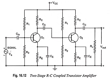
The emitter bypass capacitor CE, offers low reactance path to the signal. If it is not present, then the voltage drop across RE will reduce the effective voltage available across the base-emitter terminals (the input voltage) and thus reduces the gain.
The coupling capacitor CC transmits ac signal but blocks the dc voltage of the first stage from reaching the base of the second stage. Thus the dc biasing of the next stage is not interfered with. For this reason, the coupling capacitor CC is also called the blocking capacitor.
Operations of RC Coupled Transistor Amplifier:
When ac signal is applied to the base of the first amplifier, it appears in the amplified form across collector load RC. The amplified signal developed across RC is transmitted to the base of next stage of the amplifier through coupling capacitor CC. This is further amplified by the next stage and so on. Thus the cascade stages amplify the signal and thus the overall gain is considerably increased. The phase of output is the same as that of input because the phase is reversed twice by two transistors as they are in CE configuration.
It may be mentioned here that the overall gain is less than the product of the gains of individual stages. This is because when
a second stage is made to follow the first one, the effective load resistance of the first stage is reduced because of the shunting effect of the input resistance of the second stage. This reduces the gain of the stage which is loaded by the next stage. For example, in a 4-stage amplifier the gains of first three stages will be reduced due to loading effect of the subsequent stage. However, the gain of final or last stage (4th stage in this case) which has no loading effect of subsequent stage, remains unaffected. Thus the overall gain shall be less than the product of the gains of four stages.
Analysis:
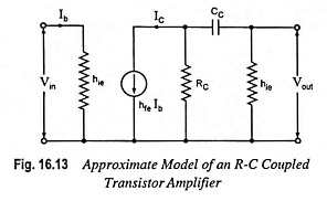
For drawing approximate model of the circuit shown in Fig. 16.12, following assumptions are made.
- hre is so small that the voltage source hre Vout can be neglected.
- 1/hoe is so large that it can be considered as an open circuit.
- The bias resistors R1 and R2 are very large in comparison to hie.
- The reactance of emitter bypass capacitor CE for any given input frequency is so small that parallel combination of RE and CE can be considered as a short circuit.
The approximate model drawn with the above assumptions is shown in Fig. 16.13.
For the purpose of analysis the entire frequency range may be divided into the following three categories.
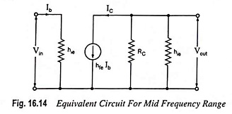
(a) Mid Frequency Range: At mid frequencies, the impedance offered by the coupling capacitor CC is so small that it can be effectively considered as a short circuit and its effect can be neglected. Equivalent circuit for mid frequency range is given in Fig. 16.14 and its Thevenin’s equivalent circuit is given in Fig. 16.15.
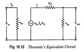
From circuit shown in Fig. 16.15

So Current gain,
![]()
Output Voltage,
![]()
Input Voltage,
![]()
So Voltage gain
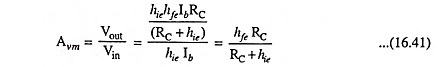
From Eqs. (16.39) and (16.41) it is obvious that current and voltage gains are equal.
(b) Low Frequency Range: In low frequency range, the impedance offered by coupling capacitor CC is comparable to the collector resistance RC. It largely affects the current amplification. Therefore, it becomes necessary to include it in the equivalent circuit, as shown in Fig. 16.13
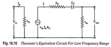
Thevenin’s equivalent circuit is given in Fig. 16.16. From circuit shown in Fig. 16.16
Current,
![]()
so current gain,
![]()
Output voltage,
![]()
Input voltage
![]()
So voltage gain,
![]()
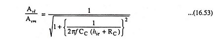
The magnitude of Avl is given by
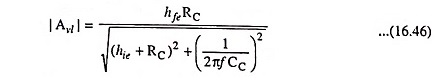
From Eq. (16.46) it is obvious that in the low frequency range voltage gain decreases with the decrease in frequency.
(c) High Frequency Range: In high frequency range, the reactance offered by coupling capacitor CC is very small and it may be considered as a short circuit.
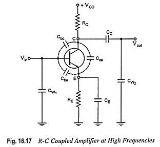
The important factor that comes into picture at high frequencies is the interelectrode capacitances. These capacitances are due to formation of depletion layers at the junctions. The interelectrode capacitances are shown by dotted lines in Fig. 16.17. The capacitance Cbc between the base and collector connects the output with the input. Because of this, negative feedback takes place in the circuit and gain is reduced.
The feedback effect increases with the increase in frequency because with the increase in frequency reactive impedance of the capacitor decreases. The capacitance Cbe, between the base and emitter, offers a low impedance path at the input side at high frequencies. This reduces the input impedance of the device, and consequently effective input signal is reduced. Thus gain falls. Similarly, the capacitance Cce produces a shunting effect at high frequencies on the output side. It is noteworthy point that Cbc is the most important capacitance because feedback takes place from output circuit to input circuit through this capacitance. This is known as Miller effect. Besides these capacitances, there are wiring capacitances CW1 and CW2, as shown in Fig. 16.17. These are the capacitances between the connecting wires of the circuit and ground.
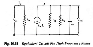
It can be shown that Cbe and Cbc may be replaced with a single capacitor Cd across the input resistance hie of the transistor. The value of shunt capacitance Cd in the input circuit of the first stage is small because it depends on the output impedance of the first transistor, which is small. But in the output circuit of the first stage Cd is increased by stray capacitance of the wiring. The reactance 1/ωCd will have appreciable shunting effect on R2 and hie. The equivalent circuits are given in Figs. 16.18 and 16.19.
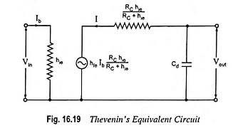
From Thevenin’s equivalent circuit shown in Fig. 16.19,
Current,
![]()
So current gain,
Output voltage,
![]()
Input voltage,
![]()
Therefore, Voltage gain,
![]()
The magnitude of Avh is given by
From Eq. (16.50) it is obvious that with the increase in input frequency the magnitude of voltage gain falls off.
Lower Cutoff Frequency:
The lower cutoff frequency, f1 may be defined as the frequency at which the magnitude of the voltage gain in the low frequency range falls off to 1/√2 or 0.707 times the maximum gain in the mid frequency range. Thus at f = f1
![]()
From Eq. (16.46) the magnitude of Avl,
![]()
and from Eq. (16.41), the magnitude of Avm,
![]()
From Eqs. (16.51) and (16.52)
If f1 is the lower cutoff frequency, then
![]()
From Eqs. (16.53) and (16.54), we have
![]()
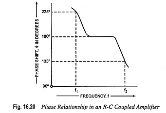
So the total phase shift of the voltage gain Avl in the low frequency range is given by
![]()
From above equation it is obvious that with the decrease in frequency θl increases and at f = f1
![]()
Upper Cutoff Frequency:
The upper cutoff frequency f2 may be defined as the frequency at which the magnitude of the voltage gain in the high frequency range falls off to 1/√2 or 0.707 times the magnitude of the gain in the mid frequency range. Thus at f = f2
![]()
From Eq. (16.50), the magnitude of Avh,
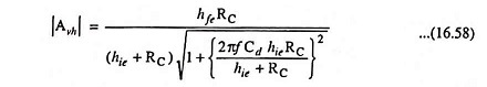
From Eqs. (16.52) and (16.58) we have
![]()
If f2 is the upper cutoff frequency then
![]()
or Upper cutoff frequency,

From Eqs. (16.59) and (16.60)
![]()
Φh decreases with the increase in input frequency f. The variation of total phase shift between input and output voltages with frequency is shown in Fig. 16.20.
Frequency Response Curve:
The frequency response curve of a typical RC Coupled Transistor Amplifier is shown in Fig. 16.21.
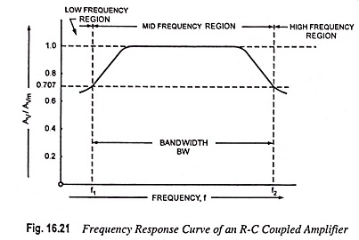
In mid frequency range (50 Hz – 20 kHz), the voltage gain of the amplifier is constant, as is obvious from the analysis. With the increase in the frequency in this range, the reactance of the coupling capacitor CC reduces thereby increasing the gain but at the same time lower capacitive reactance causes higher loading resulting in lower voltage gain. Thus the two effects cancel each other and uniform gain is obtained in mid frequency range.
At low frequencies (below 50 Hz) higher capacitive reactance of coupling capacitor CC allows very small part of signal to pass from one stage to the next and also because of higher reactance of emitter bypass capacitor CE, the emitter resistor RE is not effectively shunted. Thus the voltage gain falls off at low frequencies.
At high frequencies (exceeding 20 kHz), the gain of the amplifier decreases with the increase in frequency. Several factors are responsible for this reduction in gain. At high frequencies, the reactance of coupling capacitor CC becomes very small and CC behaves as a short circuit. This increases the loading of next stage and reduces the voltage gain. At high frequencies, capacitive reactance of base-emitter junction is low and so the base current is increased and current gain factor β is reduced. At high frequencies, the interelectrode capacitance Cbc connects the output circuit to the input circuit. Thus negative feedback takes place and the gain is reduced. Besides interelectrode capacitances, there are wiring capacitances CW1, and CW2 and input capacitance Cin of the next stage. The effect of the capacitances CW1, CW2 and input capacitor Cin of the next stage can be represented by a single shunt capacitance given as
![]()
The output section of the amplifier is shown in Fig. 16.22 from the ac point of view, for high frequency considerations. The capacitance Cs is the equivalent shunt capacitance as given by Eq. (16.64). In figure coupling and bypass capacitors CC and CE are not shown as they effectively represent short circuits at high frequencies.
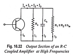
From circuit shown in Fig. 16.22, it is obvious that collector current Ic is made up of three currents I1, I2 and I3. With the increase in frequency of the input signal, the reactive impedance of the shunt capacitance Cs decreases, being inversely proportional to frequency, and as a result the current I2 through this capacitance Cs increases. This reduces both currents I1 and I3 since total current Ic = (l1 + l2 + l3) is almost constant. The output voltage Vout being the product of l3 and R (i.e. I3R) decreases. Thus higher the frequency, the lower is the impedance offered by Cs and lower will be the output voltage Vout.
Bandwidth:
Frequency response curve of an RC Coupled Transistor Amplifier is shown in Fig. 16.21. The cutoff frequencies f1 and f2 are marked in the figure. The difference of the two frequencies (upper cutoff frequency f2 and lower cutoff frequency f1) is called the bandwidth (BW)
![]()
when the bandwidth (BW) is multiplied by the gain at mid frequencies, gain-band width (GBW) is obtained.
Advantages of RC Coupled Transistor Amplifier:
Excellent frequency response (constant gain over the audio-frequency range, the most important region for speech, music etc.), cheaper in cost (resistors and capacitors used are very cheap) and very compact circuit (resistors and capacitors used being small and extremely light).
Disadvantages of RC Coupled Transistor Amplifier:
Low voltage and power gain due to low resistance presented by the input of each stage to the preceding stage, tendency of becoming noisy with age, particularly in moist climates, and poor impedance matching due to difference in impedances of the RC Coupled Transistor Amplifier output and that of the speaker.
Applications of RC Coupled Transistor Amplifier:
The RC Coupled Transistor Amplifier are widely used as voltage amplifiers (i.e. in the initial stages of public address systems) because of their excellent audio fidelity over a wide range of frequency. However, because of poor impedance matching, this type of coupling is rarely employed in the final stages.