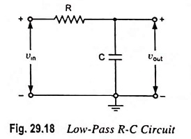
Low Pass RC Circuit Diagram, Derivation and Application:
The Low Pass RC Circuit is shown in Fig. 29.18. In a Low Pass RC Circuit, the output voltage vout is taken across the capacitor. Resistance offers fixed opposition. Since the reactance offered by the capacitor C falls with the increase in frequency, low frequency signal develops across the capacitor but signal of frequency above cutoff frequency f2 develops negligible voltage across capacitor C. At zero frequency, the capacitor acts as an open circuit and output is same as input. However, with the increase in frequency, the capacitive reactance decreases and so the output voltage. At infinite frequency, the capacitive reactance of the circuit will be zero, and therefore, output voltage will also be zero. Since it passes low frequency signals and blocks the high frequency signals, it is called the low-pass circuit.
Response of Low Pass RC Circuit to Standard waveforms:
1. Sinusoidal Input:
For a sinusoidal input the waveshape of the output will remain the same; the output will differ only in amplitude and phase angle depending on frequency of the input signal. So only gain of the circuit needs consideration.

The current through the circuit is given as

Output voltage,

So gain
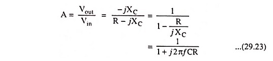
From the above equation it is obvious that for a circuit, the gain A depends upon the frequency of the input signal.
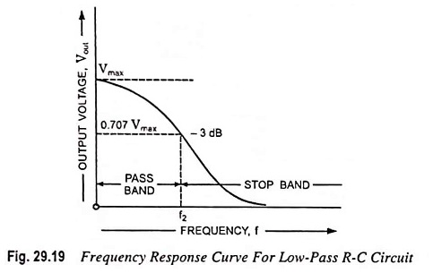
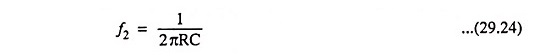
The frequency response curve for the circuit is given in Fig. 29.19. From frequency response curve it is obvious that all frequencies below cutoff frequency f2 are passed while those above are attenuated. At cutoff frequency R = XC, the phase angle is 45° and output power is half of the input power. The output voltage is 0.707 times the maximum value of voltage Vmax. The cutoff frequency f2 is given as
Substituting 1/2πRC = f2 in Eq. (29.23) we have

Now magnitude of A and phase angle θ are given as

and phase angle

As

When

f2 is also known as high 3-dB frequency
f = f2 also implies that

So f2 is the frequency at which capacitive reactance XC is equal to the resistance of the circuit.
2. Step Input:
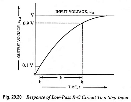
At instant t = 0–, since the input is zero, the output is also zero. At instant t = 0, the input suddenly becomes V. Since the voltage across a capacitor cannot change instantaneously, the output voltage remains zero. At t = 0+, the input voltage remains unchanged at V, the capacitor starts charging exponentially to voltage V and the output is the same as the capacitor voltage. The response of the Low Pass RC Circuit to a step input is shown in Fig. 29.20. The output voltage is given as
![]()
The time taken by the capacitor to rise from 0.1 to 0.9 of its final value is called the rise time. It indicates how fast the circuit responds to a discontinuity in voltage.
Let the time required for output voltage to attain one-tenth of its final value be t = t1. So at t = t1
Now if t2 is the time required by the capacitor to attain 0.9 times its final value, then
So rise time, tr = t2 – t1 = 2.3 CR – 0.1 CR
Since bandwidth of a circuit, Δf = f2 – f1.
As the lower cutoff frequency f1 for the circuit is zero, therefore, Bandwidth Δf = f2.
Thus rise time is proportional to the time constant τ and inversely proportional to the bandwidth or upper 3-dB frequency.
3. Pulse Input:
The response to a pulse, for times less than the pulse width tp is the same as that for a step input because pulse signal is same as step input for t < tp. However, at the end of the pulse, as the input becomes zero, the output also drops exponentially to zero. The reason is that capacitor voltage falls exponentially to zero, as the input becomes zero.
Thus output for pulse input is given as

At t = tp,

At t = tp, input voltage becomes zero but since the voltage across a capacitor cannot change instantaneously, output remains the same as it is at t = tp. After that capacitor starts getting discharged through resistance R and voltage across it drops exponentially to zero. Hence output voltage for t > tp.
![]()
The above equation is discharging equation of capacitor delayed by time tp. Hence output voltage must be decreasing towards zero for t > tP. This is illustrated in Fig. 29.21.
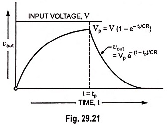
It shows that output voltage will always extend beyond pulse width tp. This is because the charge stored on capacitor during pulse cannot leak off instantaneously.
It is also observed from Fig. 29.21 that output shape is different from that of input i.e., there is distortion. Distortion may be reduced by making rise time much smaller than pulse width tp. For a circuit having f2 equal to 1/tp, tr = 0.35 tp. For this value of tr output will be of the shape shown in Fig. 29.22, which is not exact but approximately reproduction of the input.
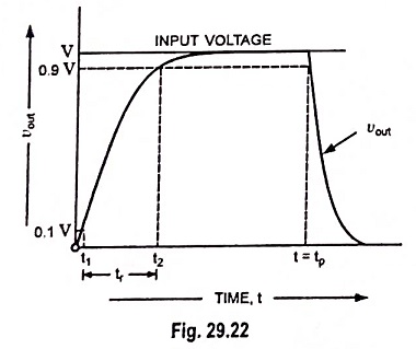
As a thumb rule it can be said :
A pulse shape will be preserved if the 3-dB frequency is approximately equal to the reciprocal of the pulse width (PW).
Thus to pass a 0.2 μs pulse reasonably well needs a circuit with an upper cutoff frequency of the order of 5 MHz.
4. Square-Wave Input:
Consider a periodic waveform whose instantaneous value is constant at V’ w.r.t. ground for a time T1 and then changes abruptly to V” for a time T2. A reasonable reproduction of the input is obtained if the rise time tr is small compared with the pulse width. The steady-state response is drawn in Fig. 29.23 (b). If the time constant RC is comparable with the period of input square-wave, the output will have the appearance, as illustrated in Fig. 29.23 (c). If the time constant is very large compared with the input wave period, the output will consist of exponential sections which are essentially linear as illustrated in Fig. 29.23 (d).
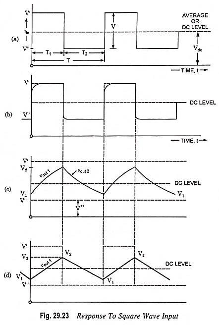
The input appears pulses of opposite polarity and added alternately. Like pulse output for time 0 < t < T1, for square-wave input also output is vout = V′ (1 – e-t/RC) and at t = T1 it is V′ (1 – e-T1/RC) if capacitor is initially uncharged.
Since for succeeding cycles capacitor may remain charged to some value at the beginning of the new cycle, so taking a generalized case, and then analyzing the circuit shown in Fig. 29.18 for 0 < t <T1.
Initially charged capacitor is equivalent to an uncharged capacitor in series with a voltage source of magnitude and polarity equal to that initial charge. This is illustrated in Fig. 29.24.
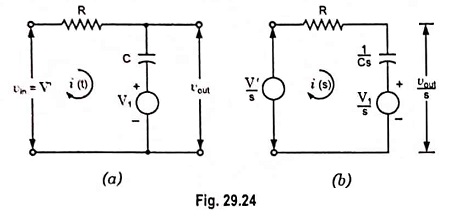
Let at t = 0+ capacitor is initially charged to a voltage V1 and for 0 < t < T1
Input voltage, vin = V′
The circuit shown in Fig. 29.18 is redrawn for time 0 < t < T1 and is shown in Fig. 29.24 (a) and its Laplace transform is shown in Fig. 29.24 (b).
Applying Kirchhoff’s voltage law to the circuit we have
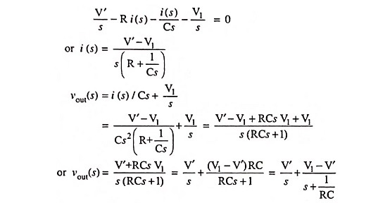
Taking inverse Laplace we have
![]()
So output voltage for 0 < t < T1
![]()
Similarly for T1 ≤ t ≤ T2, if initial voltage across capacitor is V2 and input voltage is constant at V” and output voltage = Vout2 (say)

Then at t = T1,

and at t = T1 + T2,

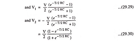
For symmetrical wave
![]()
Therefore,

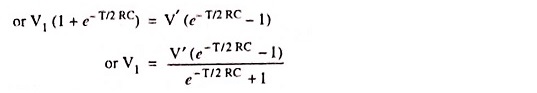
If peak-to-peak voltage of input square-wave is V, then V′ = V/2
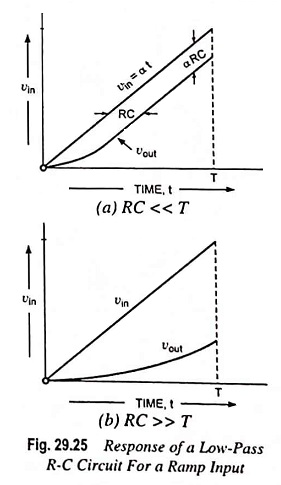
5. Ramp Input:
A waveform which is zero for t < 0 which increases linearly with time for t > 0, v = αt, is known as a ramp or sweep voltage. Assume that the Low Pass RC Circuit shown in Fig. 29.18 is excited by a ramp input vin(t) = αt where α is the slope of the ramp.
Since at any instant input voltage vin is equal to the pd across resistor plus pd across the capacitor,

Differentiating above equation w.r.t. time we have
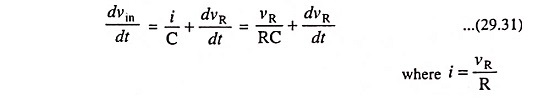
The above equation has the solution for vR = 0 at t = 0
![]()
The voltage across the capacitor is
When the time constant τ = RC is very small in comparison to the total ramp time T, the ramp will be transmitted with minimum distortion. It is seen from Fig. 29.25 (a) that the output follows the input but is delayed by one time constant RC from the input (except near the origin) where there is a distortion. If the time constant is large in comparison to the sweep duration i.e., RC >> T, the output will be highly distorted, as depicted in Fig. 29.25 (b).
The transmission error is defined as the difference between input and output divided by the input at t = T. For RC << T, we find transmission error
where f2 is the upper 3-dB frequency.
By expanding the exponential term in Eq. (29.33), we find
This shows that a quadratic response is obtained for a linear input and thus the circuit acts as an integrator for RC >> T.
6. Exponential Input:
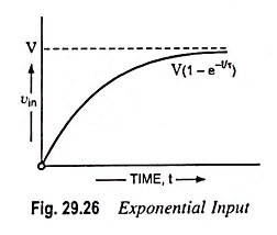
When an exponential input
![]()
shown in Fig. 29.26 is applied to Low Pass RC Circuit shown in Fig. 29.18, Eq. (29.31) becomes
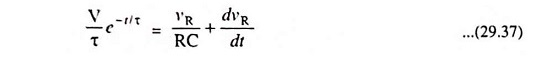
Defining x and n by

The solution of Eq. (29.37), subjected to the condition that initially the voltage across the capacitor is zero, is given by the expression

Hence the voltage across the capacitor is equal to the difference of input voltage less voltage across the resistor. Thus
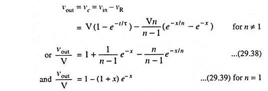
The parameters x and n are defined by x ≡ t/τ and n ≡ RC/T.
Above Eqs. (29.38) and (29.39) give the voltage across the capacitor of a Low Pass RC Circuit when excited by an exponential input of rise time tr1 = 2.2τ.
If an exponential of rise time tr1 is passed through a Low Pass RC Circuit with rise time tr2 = 2.2 RC, the rise time of the output waveform tr will be given by an empirical relation,
![]()
This is same as the rise time obtained when a step is applied to a cascade of two circuits of rise times tr1 and tr2 assuming that the second circuit does not load the first one.
Applications:
R-C circuits with time constant larger than the time period of the input wave (i.e., RC >> T) are used as bypass capacitors. Low-pass filters are also employed in generation of triangular and ramp waveforms. It also finds application in discrimination between pulses of different lengths.
Integrators are almost invariably preferred over differentiators in analog computer applications. The reasons are given below:
- Since the gain of an integrator falls with the increase in frequency whereas the gain of the differentiator increases nominally linearly with frequency, it is easier to stabilize the former than the latter with respect to spurious oscillations.
- An integrator is less sensitive to noise voltages than a differentiator because of its limited bandwidth.
- The amplifier of a differentiator may get overloaded in case the input waveform changes very rapidly.
- It is more convenient to introduce initial conditions in an integrator.