Breakdown Voltage of PN Junction Diode:
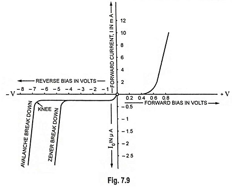
When an ordinary P-N junction diode is reverse biased, normally only very small reverse saturation current flows. This current is due to movement of minority carriers. It is almost independent of the voltage applied. However, if the reverse bias is increased, a point is reached when the junction breaks down and the reverse current increases abruptly, as shown in Fig. 7.9. This current could be large enough to destroy the junction.
If the reverse current is limited by means of a suitable series resistor, the power dissipation at the junction will not be excessive, and the device may be operated continuously in its breakdown region to its normal (reverse saturation) level. It is found that for a suitably designed diode, the Breakdown Voltage of PN Junction Diode is very stable over a wide range of reverse currents. This quality provides the breakdown diode many useful applications as a voltage reference source.
The critical value of the voltage, at which the breakdown of a P-N junction diode occurs, is called the breakdown voltage. The Breakdown Voltage of PN Junction Diode depends on the width of the depletion region, which, in turn, depends on the doping level. The junction offers almost zero resistance at the breakdown point.
There are two mechanisms by which breakdown can occur at a reverse-biased P-N junction : avalanche breakdown and zener breakdown.
The minority carriers, under reverse-biased conditions, flowing through the junction acquire a kinetic energy which increases with the increase in reverse voltage. At a sufficiently high reverse voltage (say 5 V or more), the kinetic energy of minority carriers becomes so large that they knock out electrons from the covalent bonds of the semiconductor material. As a result of collision, the liberated electrons in turn liberate more electrons and the current becomes very large leading to the breakdown of the crystal structure itself. This phenomenon is called the avalanche breakdown. The breakdown region is the ‘knee’ of the characteristic curve. Now the current is not controlled by the junction voltage but rather by the external circuit.
Under a very high reverse voltage, the depletion region expands and the potential barrier increases leading to a very high electric field across the junction. The electric field will break some of the covalent bonds of the semiconductor atoms leading to a large number of free minority carriers, which suddenly increase the reverse current. This is called the zener effect. The breakdown occurs at a particular and constant value of reverse voltage called the breakdown voltage. It is found that zener breakdown occurs at electric field intensity of about 3 x 10⁷ V/m.
Either of the two (zener breakdown or avalanche breakdown) may occur independently, or both of these may occur simultaneously. Diode junctions that break down below 5 V are caused by zener effect. Junctions that experience breakdown above 5 V are caused by avalanche effect. Junctions that break down around 5 V are usually caused by combination of two effects. The zener breakdown occurs in heavily doped junctions (P-type semiconductor moderately doped and N-type heavily doped), which produce narrow depletion layers. The avalanche breakdown occurs in lightly doped junctions, which produce wide depletion layers.
With the increase in junction temperature zener breakdown voltage is reduced while the avalanche breakdown voltage increases. The zener diodes have a negative temperature coefficient while avalanche diodes have a positive temperature coefficient. Breakdown Voltage of PN Junction Diode around 5 V have zero temperature coefficient.
The breakdown phenomenon is reversible and harmless so long as the safe operating temperature is maintained.
Despite the fact that avalanche and zener constitute two types of breakdown diodes, the name zener is commonly applied to both types of diodes.