Leakage Current in a Transistor and Breakdown Voltage:
Leakage Currents: In CB circuits shown in Fig. 10.77, if emitter current is made zero, the B-C junction still remains reverse biased and therefore, a reverse-bias leakage current exists in this junction, and this current corresponds to the reverse-bias saturation current in a diode. The direction of these reverse-bias leakage currents is the same as that of collector currents. The collector leakage current in the common-base configuration is denoted by ICBO, and is the collector-base leakage current when the emitter is open-circuited. The leakage current in a transistor is shown in Fig. 10.77(a).
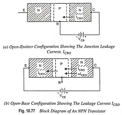
Another leakage current in a transistor can exist between the emitter and collector with the base terminal open-circuited [Fig. 10.77(b)]. The current component ICBO is the normal leakage current in the reverse-biased B-C PN junction. This current component causes the base voltage to increase, which forward biases the base-emitter junction and induces the base-emitter current ICBO. The current component αICBO is the normal collector current resulting from the emitter current ICBO. We may write
![]()
The above relationship indicates that the open-base configuration produces different characteristics than the open-emitter configuration.
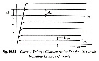
When the transistor is biased to operate in the forward-active mode, the various leakage current in a transistor still exist. Common-emitter current-voltage characteristics are depicted in Fig. 10.78, in which leakage currents have been included, A dc beta βdc or dc common-emitter current gain may be given as
![]()
where the collector current IC2 includes the leakage current as shown in the figure. An ac β, βac is defined as
![]()
The definition of beta excludes the leakage current as shown in the figure.
If the leakage currents in a transistor are negligible, the two values of beta are equal (i.e. βac = βdc).
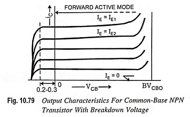
Breakdown Voltage : Common-Base Characteristics. Figure 10.79 shows the output characteristics for common base NPN transistor with breakdown voltage. Consider the curve for iE = 0 the emitter terminal is effectively opened. The collector-base junction breakdown voltage is indicated as BVCBO. This is simplified figure in that it shows breakdown occurring abruptly at BVCBO. For the curves iE > 0, breakdown actually begins earlier. The carriers flowing across the junction initiate the breakdown avalanche process at somewhat lower voltages.
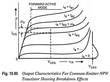
Breakdown Voltage : Common-Emitter Characteristics. Figure 10.80 shows the output characteristics of a common-emitter NPN transistor, for various constant base currents, and an ideal breakdown voltage of BVCBO. The value of BVCBO is less than the value of BVCBO because BVCBO includes the effects of the transistor action, while BVCBO does not. The same effect was observed in the ICBO leakage current.
The breakdown voltage characteristics for the two configurations are also different. The breakdown voltage for the open-base case is given by
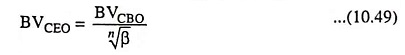
where n is an empirical constant usually in the range of 3 to 6.
Breakdown may also occur in the base-emitter junction if a reverse-bias voltage is applied to that junction. The junction breakdown voltage decreases with the increase in doping concentrations. Since the emitter doping concentration is usually substantially larger than the doping concentration in the collector, the base-emitter junction breakdown voltage is normally much smaller than that of the collector-base junction. Typical base-emitter junction breakdown voltage values are in the range of 6 to 8 V.