Transistor Lead Identification and Testing:
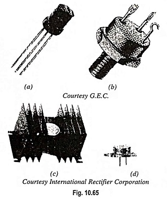
Transistor Lead Identification and Testing – After the transistor has been manufactured, as already discussed, leads of, typically, gold, aluminium, or nickel are then attached and the entire structure is encapsulated in a container such as that given in Fig. 10.65. Those with the studs and heat sinks are high power devices, whereas those with small can (top hat) or plastic body are low-to-medium power devices.
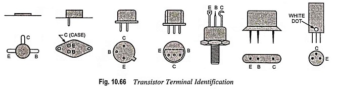
Whenever possible, the transistor casing will have some marking to indicate which leads are to be connected to emitter, collector, or base of a transistor. A few of the methods commonly employed are indicated in Fig. 10.66.
Sometimes we come across a transistor whose specifications are not known, even transistor type number is obliterated from its body and reference data book is not available. In such circumstances testing of transistors becomes necessary. Here we will describe tests for determination of type of transistor (PNP or NPN type) and for Transistor Lead Identification of transistor terminals.
1. Test for Determination of Transistor Type (PNP or NPN Type): The circuit for test to distinguish between PNP and NPN type transistors is given in Fig. 10.67 (a). This circuit makes use of two germanium rectifier semiconductor diodes and two LEDs and a heavy series resistor RS in order to limit the current in the circuit. Two leads of the tester are brought out as 1 and 2. When a resistor R is placed in the circuit, the current passes through the circuit for both the half cycles of the input voltage wave but LEDs glow alternately. However, both of the LEDs appear glowing continuously because supply frequency is quite high (50 Hz).
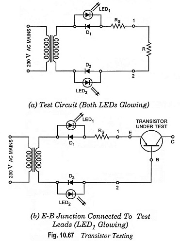
Now let the emitter-base junction of a PNP transistor is connected across the test leads 1 and 2, as shown in Fig. 10.67 (b). In this case, current does not flow through the circuit during the half cycles when the E-B junction is reverse biased. During the half cycles in which E-B junction is forward biased, current flows through LED1, series resistor RS, E-B junction and diode D2. Thus only LED1 glows. This test indicates that the terminal connected to the test lead 1 is P-type and that connected to test lead 2 is N-type. Thus P- and N-type terminals of a P-N junction are identified, LED1 will also glow if C-B junction of PNP transistor is connected across test leads 1 and 2. However, none of the LEDs will glow when test leads are connected to the collector and emitter of the transistor because in this case base is open circuited.
It is thus seen that only one LED glows when the test leads are connected either across E-B junction or C-B junction i.e., between these two pair of terminals, the common terminal must be the base terminal and the remaining must be emitter and collector terminals. In case the common terminal (the base) is N-type, the transistor is obviously PNP type. In the other case, when the common terminal is P-type, it is an NPN type transistor. This test cannot distinguish between terminals E and C.
Glowing of both LEDs indicate a short-circuited pair of terminals (i.e., faulty transistor).
For Transistor Lead Identification of emitter and collector terminals another test, which is described below, will have to be conducted.
2. Transistor Lead Identification of Emitter and Collector Terminals of a Transistor: Once the type (PNP or NPN) of transistor is known and base terminal is identified, emitter and collector terminals can be identified by an ohmmeter or a multimeter. We know that for a transistor in the active region the base-to-emitter junction is forward biased and the base-to-collector junction is reverse biased. Essentially, therefore, the forward biased base-to-emitter junction should register a relatively low resistance, whereas the reverse biased base-to-collector junction shows a much higher resistance.
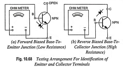
For an NPN transistor, the forward biased junction (biased by the internal supply in the resistance mode) from base to emitter should be checked as shown in Fig. 10.68 (a) and result in an indication that will typically fall in the range of 100 Ω to a few kilohms. The reverse biased base-to-collector junction (again reverse biased by the internal supply) should be checked as shown in Fig. 10.68 (b) with an indication typically exceeding 100 kΩ. While testing a PNP transistor, the ohmmeter leads must be reversed for each junction. The test result will be the same. Obviously, a large or small resistance in both directions (reversing the leads) for either junction of an NPN or PNP transistor indicates a faulty device.
When a multimeter is used in its ohmmeter function, the terminal polarity should be checked with a voltmeter. Transistor base-emitter junctions usually do not survive reverse bias voltage in excess of 5 V. Therefore, when testing transistors, the ohmmeter should be used only in medium and low resistance ranges, to avoid the 15 V internal supply sometimes employed with high resistance ranges.