Large Signal Tuned Amplifier – Operation and its Equivalent Circuit:
Tuned amplifier circuits are for class A operation and their use is limited to applications in which RF signal has low power levels such as in radio receivers. Such amplifiers are not suitable for applications involving larger RF power, because of lower efficiency of class A operation, such as for excitation of transmitting antenna. For such applications, large signal tuned amplifiers are employed because they are operated in class C operation that has a very high efficiency and is capable of delivering more power in comparison to that of class A operation.
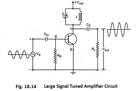
Large signal tuned amplifier circuit is shown in Fig. 18.14. The resonant tuned circuit is tuned to the frequency of the input signal. When the circuit has a high Q factor (i.e., inductive reactance of inductor is much larger than its resistance), parallel resonance occurs at approximately frequency given by

At the resonant frequency, the impedance of the parallel resonant circuit is very large and is purely resistive. (This approximation assumes that the Q of the circuit is greater than 10, a condition usually satisfied in tuned amplifiers). When the large signal tuned amplifier circuit is tuned to the resonant frequency, the voltage across load resistance RL is maximum and sinusoidal.
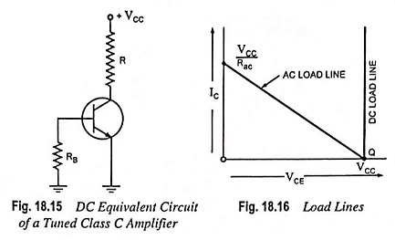
DC equivalent circuit of large signal tuned amplifier circuit is shown in Fig. 18.15. It is to be noted that there is no bias applied to the transistor. Therefore, its Q point is at cutoff on the dc load line. Since there is no dc bias, so VBE is zero. This means that no collector current can flow until the input signal attain a value greater than approximately 0.7 V. DC collector resistance R is the dc resistance of the RF inductor L, typically a few ohms.
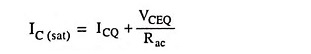
Load Lines: The dc load line appears to be almost vertical, as shown in Fig. 18.16. This is because the dc collector resistance R is very small. There is no danger of thermal runaway because the transistor has no current aside from leakage. The Q point is located at cutoff with no risk of thermal runaway.
For a CE amplifier,
and
![]()
and for a class C amplifier shown in Fig. 18.14 ICQ = 0 and VCEQ = VCC.
Therefore, the foregoing equations reduce to
AC load line is shown in Fig. 18.16. When the transistor is conducting, its operating point swings upward along the ac load line. As before, Rac is the ac resistance seen by the collector. Therefore ac saturation current in a class C amplifier is VCC/Rac, and the maximum voltage swing is VCC.
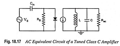
AC Equivalent Circuit: Approximate ac equivalent circuit, assuming Q of the resonant circuit to be greater than 10, is shown in Fig. 18.17. In this equivalent circuit, the series resistance of the inductor is lumped into the collector resistance. In a class C amplifier, the input capacitor is part of a negative dc clamper. On the input side of a class C amplifier, therefore, the signal is negatively clamped. On the output side, the collector current source drives a parallel resonant tank circuit. At resonance, the peak-to-peak load voltage attains a maximum.
AC Collector Resistance: Any coil or inductor has some series resistance R. Although in schematic diagrams, it is never shown as a separate component. The Q factor of the inductor is given as QL = XL/R
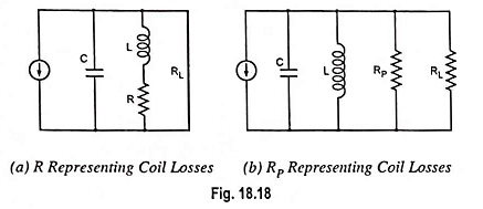
where XL and R are the inductive reactance and resistance of the inductive coil and QL is quality factor of the coil. The quality factor Q for the whole circuit is less than that for the coil because it includes the effect of load resistance as well as the coil resistance. The series resistance of the inductor, however, can be replaced by a parallel resistance RP, as illustrated in Fig. 18.18 (b). This equivalent resistance is given by an approximate expression RP = QLXL. For XL >> 10, this relation gives an error of less than 1%.
In Fig. 18.18 (b), it is to be noted that all the losses in the coil are now represented by the parallel resistance RP, series resistance R no longer exists in the equivalent circuit. Because of this, XL neutralize XC at resonance, leaving only RP in parallel with RL. Thus ac resistance seen by the collector at resonance is given as
![]()
and the quality factor Q of the circuit is given as
![]()
Since the overall Q is 10 or more, the operation is narrowband. Also, since the Q of the coil is 50 or more, most of the ac load is delivered to the load resistor and only a small amount of power is wasted in the coil resistance.
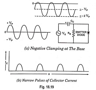
DC Clamping: In the Fig. 18.19 (a), the input signal charges the coupling capacitor to approximately VP with the polarity shown. During the positive half cycles, the emitter diode conducts briefly at the peaks; this replenishes any capacitor charge lost during the cycle. During the negative half cycles, the only discharge path is through RB. As long as the period T of the input signal is much smaller than the time constant RBC, the capacitor loses only a small amount of its charge. For replenishment of the lost capacitor charge, the base voltage must swing slightly above 0.7 V to turn on the emitter diode briefly at each positive peak, as shown in Fig. 18.19 (a). The conduction angle of the base and collector current, therefore, is much less than 180°. This is why the collector current is a train of narrow pulses, as shown in Fig. 18.19 (b).
Duty Cycle: The brief turn-on of the emitter diode at each positive peak produces narrow pulses of collector current. With such pulses, it is convenient to use the duty cycle, defined as
![]()
where D is duty cycle, W is width of pulse and T is period of pulses.
For instance, the pulse width shown on an oscilloscope is of 0.25 μs and a period shown is 1.75 μs, the duty cycle is
![]()
Filtering of Harmonics: As discussed earlier, nonsinusoidal wave consists of fundamental frequency f and its harmonics i.e., 2f, 3f, 4f and so on. In Fig. 18.20 (a), the collector current source drives the resonant tank circuit with the nonsinusoidal current shown in Fig. 18.19 (b). If the tank circuit is resonant to the fundamental frequency, then all the harmonics are filtered out, and the load voltage is sinusoidal of fundamental frequency, as shown in Fig. 18.20 (b).
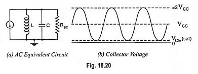
As discussed earlier, the maximum voltage swing along the ac load line is approximately VCC. Therefore, under full-signal conditions, the load voltage swings from approximately VCE (sat) to 2 VCC. Thus the ac output of a class C amplifier is ≡ 2 VCC because VCE (sat) is about equal to zero.
The class C amplifier is rather unusual. First it clamps the input signal negatively to get highly distorted current pulses. Then it makes use of a high-Q resonant circuit to restore the fundamental frequency. This improves the stage efficiency. Furthermore, because of the narrow current pulses, the transistor power dissipation is lower than with class A or class B. The overall effect is less current drain, which means a higher stage efficiency. The efficiency of class C approaches 100 per cent.
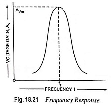
Frequency Response and Bandwidth: The frequency response curve of a class C tuned amplifier is shown in Fig. 18.21. Voltage gain attains maximum value at the resonant frequency. On both sides of the resonant frequency, the voltage gain decreases, as illustrated in Fig. 18.21. The higher the Q of the circuit, the faster the gain drops off on either side of the resonant frequency.
The bandwidth of the tuned amplifier is given as
![]()
From above relation it is obvious that with a large Q, a small bandwidth, equivalent to sharp tuning, is obtained. Class C amplifiers always have a circuit Q >> 10. This means that the bandwidth is less than 10% of the resonant frequency. For this reason, class C amplifiers are also sometimes called the narrowband amplifiers. The output of a narrowband amplifier is a large sinusoidal voltage at resonance with a rapid fall above and below resonance.