Single Input Unbalanced Output Differential Amplifier:
Single input unbalanced output differential amplifier configurations are rarely used. The reasons for this are as follows:
- This configuration is identical to the CE amplifier but it needs comparatively more components and yields less voltage gain than that of CE amplifier.
- A dc output voltage exists even in absence of any input signal.
In this configuration, an output signal can be impressed on the base of either transistor and output can be measured at either collector.
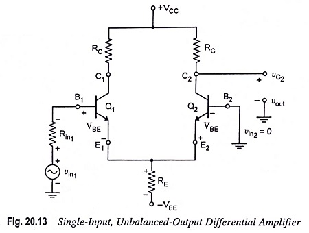
Single-input, unbalanced-output differential amplifier with input applied to the base of transistor Q1 and the output measured at the collector of transistor Q2 is shown in Fig. 20.13.
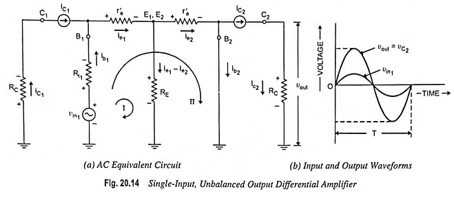
DC Analysis:
The dc analysis process and the bias equations for this configuration are also identical to those of the previous three configurations. Thus
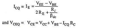
AC Analysis:
The ac equivalent circuit of the this amplifier with small signal T-equivalent models substituted for the transistors is shown in Fig. 20.14 (a).
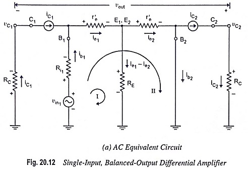
1. Voltage Gain: The ac equivalent circuit given in Fig. 20.14 (a) is similar to that given in Fig. 20.12 (a) except the way of measuring output voltage. Thus, the expressions derived for ie1 and ie2 [Eqs. (20.30) and (20.31)] for the circuit shown in Fig. 20.12 (a) hold valid for the circuit given above [Fig. 20.14 (a)]. The output voltage is given by the expression
![]()
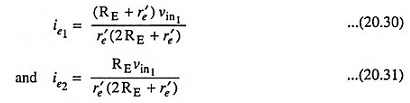
Substituting value of ie2 from Eq. (20.31) in above expression, we have
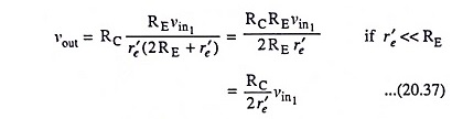
Thus, voltage gain,
![]()
The input and output waveforms are shown in Fig. 20.14(b).
2. Differential Input Resistance: The input resistance Rin of this configuration is identical to that of previous one, i.e.,
![]()
3. Output Resistance: The output resistance measured at collector C2 w.r.t. ground (Rout) is equal to the collector resistance RC [Fig. 20.14(a)].
Thus,
![]()