BJT Power Amplifier with Differential Input Stages:
Amplifier Circuit – The direct-coupled amplifier in Fig. 18-33 has a BJT Power Amplifier with Differential Input Stages constituted by transistors Q1 and Q2. It also has an intermediate stage (Q3) with a constant current load (Q4). Both pairs of output stage transistors (Q5 and Q7) and (Q6 and Q8) are in quasi-complementary configuration, instead of the usual complementary form. This arrangement helps to minimize the required supply voltage by removing the VBE of the power transistors from the VCC equation.
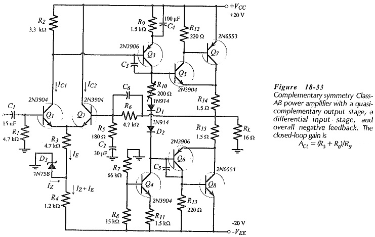
The BJT Power Amplifier with Differential Input Stages facilitates negative feedback (NFB), and the whole circuit functions like an operation amplifier. Q1 base is the noninverting input, Q2 base is the inverting input, and the junction of R14 and R15 is the output terminal. There is 100% dc NFB provided from the output via R6 to Q2 base. This keeps the output dc voltage at the same level as Q1 base, (at ground). With C2 behaving as an ac short-circuit, the ac NFB is divided by R5 and R6 to give a closed loop gain; ACL = (R5 + R6)/R5.
Zener diode D3 and resistor R4 decouple the power supply ripple on the negative supply line. The dynamic impedance of D1 combined with R4 functions as an ac voltage divider to attenuate the ripple at the emitters of Q1 and Q2. Ripple at this point is amplified just like an input signal. Capacitors C3 and C5 are frequency-compensating components.
Amplifier Design:
The design procedure for the output and intermediate stages of the circuit in Fig. 18-33 is similar to procedures already discussed. Design of the BJT Power Amplifier with Differential Input Stages is very simple. The dc collector currents for Q1 and Q2 should be larger than the peak base current for Q3, and the voltage drop across R2 is (VE3 + VBE3). Zener voltage VZ3 is any convenient level, usually around 0.5 VEE. Resistor R3 is calculated to pass IE ≈ (IC1 + IC2), and R4 must pass (IZ + IE).
Q1 bias resistor R1 is determined from earlier Equation, R6 is selected equal to R1, and R5 is calculated in terms of R6 to give the desired closed-loop gain. The impedance of C2 is made equal to R5 at the desired lower cutoff frequency (f1), so that C2 sets f1. Capacitors C1 and C4 are determined in the usual way for capacitors that are not to affect f1. An additional capacitor (C6) might be included to set the upper cutoff frequency (f2); (XC6 = R6 at f2).