Fet Tuned Amplifier – Circuit Diagram and Frequency Response:
Figure 18.11(a) depicts the circuit of an FET tuned amplifier. It uses a first-order JFET model for the 2N 5484 [IDSS = 2.41 mA, VP = -1.2 V]. Thus,
Drain current,
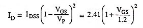
and
![]()
when gate voltage is 4.29 V
Solving for the quiescent bias values ID = 1.19 mA and VGS = – 0.35 V.
A SPICE computation provides VGS = – 0.4 V and ID = 1.24 mA. The noteworthy point is that the first order does not allow for channel length modulation.
Small signal model for operation at resonance is shown in Fig. 18.11(b). Using the computed bias current and voltage values the transconductance gm is 2.84 mA/V. The voltage gain at resonance then is 92.3 (39.3 dB).
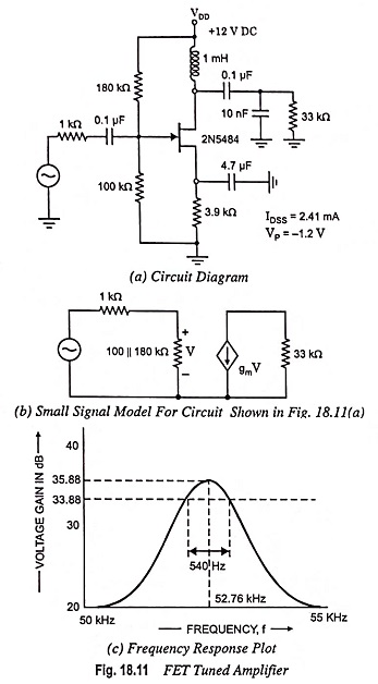
The calculated resonant frequency is 50.35 kHz. The calculated Q is approximately 104 and the 3 dB bandwidth therefore is estimated to be 484 Hz Pspice is used to provide the numerical analysis of the amplifier performance plotted below [Fig. 18.11 (c)].