Enhancement Type MOSFET – Construction, Operation and Characteristics:
Although DE-MOSFET is useful in special applications, it does not enjoy widespread use. However, it played an important role in history because it was part of the evolution towards the E-mode MOSFET, a device that has revolutionized the electronic industry. Enhancement Type MOSFET has become enormously important in digital electronics and computers. In the absence of E-MOSFETs, the personal computers (PCs) that are now so widespread would not exist.
Construction of Enhancement Type MOSFET:
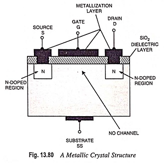
Figure 13.80 shows the construction of an N-channel E-MOSFET. The main difference between the construction of DE-MOSFET and that of E-MOSFET is that in E-MOSFET substrate extends all the way to the silicon dioxide (SiO2) and no channels are doped between the source and the drain. Channels are electrically induced in these MOSFETs, when a positive gate-source voltage VGS is applied to it.
Operation of Enhancement Type MOSFET:
As its name indicates, this MOSFET operates only in the enhancement mode and has no depletion mode. It operates with large positive gate voltage only. It does not conduct when gate-source voltage VGS = 0. This is the reason that it is called normally-off MOSFET. In these MOSFETs drain current ID flows only when VGS exceeds VGST [gate-to-source threshold voltage].
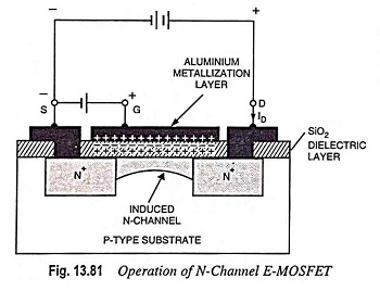
When drain is applied with +ve voltage with respect to source and no potential is applied to the gate, the two N-regions and one P-type substrate form two P-N junctions connected back to back with a resistance of the P-substrate. Both the junctions cannot be forward biased at the same time, so only an extremely small drain current i.e. a reverse leakage current flows. If the P-type substrate is now connected to the source terminal, there is zero voltage across the source-substrate junction, and the drain-substrate junction remains reverse biased. When the gate is made positive with respect to the source and the substrate, negative (i.e. minority) charge carriers within the substrate are attracted to the +ve gate and accumulate close to the surface of the substrate. As the gate voltage is increased, more and more electrons accumulate under the gate. Since these electrons cannot flow across the insulated layer of silicon dioxide to the gate, they accumulate at the surface of the substrate just below the gate.
These accumulated minority charge carriers make an N-type channel stretching from drain to source. When this occurs, a channel is induced by forming what is termed an inversion layer (N-type). Now a drain current starts flowing. The strength of the drain current depends upon the channel resistance, which in turn depends on the number of charge carriers attracted to the positive gate. Thus drain current is controlled by the gate potential.
Since the conductivity of the channel is enhanced by the +ve bias on the gate, this device is called the Enhancement Type MOSFET or E-MOSFET.
The minimum value of gate-to-source voltage VGS that is required to form the inversion layer (N-type) is termed the gate-to-source threshold voltage VGST. For VGS below VGST, the drain current ID = 0. But for VGS exceeding VGST an N-type inversion layer connects the source to drain and the drain current ID is large. Depending upon the device being used, VGST may vary from less than 1 V to more than 5 V.
JFETs and DE-MOSFETs are classified as the depletion-mode devices because their conductivity depends on the action of depletion layers. E-MOSFET is classified as an enhancement-mode device because its conductivity depends on the action of the inversion layer. Depletion-mode devices are normally ON when the gate-source voltage VGS = 0, whereas the enhancement-mode devices are normally OFF when VGS = 0.
Characteristics:
Drain characteristics of an N-channel E-MOSFET are shown in Fig. 13.82. The lowest curve is the VGST curve. When VGS is lesser than VGST, ID is approximately zero. When VGS is greater than VGST, the device turns on and the drain current ID is controlled by the gate voltage. The characteristic curves have almost vertical and almost horizontal parts. The almost vertical components of the curves correspond to the ohmic region, and the horizontal components correspond to the constant current region. Thus Enhancement Type MOSFET can be operated in either of these regions i.e. it can be used as a variable voltage resistor (VVR) or as a constant current source.
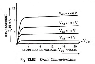
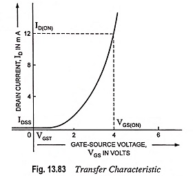
Figure 13.83 shows a typical transconductance curve. The current IDSS at VGS ≤ 0 is very small, being of the order of a few nanoamperes. When the VGS is made positive, the drain current ID increases slowly at first, and then much more rapidly with an increase in VGS. The manufacturer sometimes indicates the gate-source threshold voltage VGST at which the drain current ID attains some defined small value, say 10 μA. The current ID(ON), corresponding approximately to the maximum permissible value of drain current given on the drain characteristics and the values of VGS required to give this current VGS(ON) are also usually given on the manufacturers data sheet.
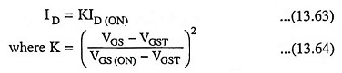
The equation for the transfer characteristic of E-MOSFETs is given as
![]()
where K, typically 0.3 mA/V2, is a property of the device construction. Note that IDSS cannot be associated with an E-MOSFET, because no drain current flows with VGS = 0 volt.
With JFETs and DE-MOSFETs, the value of IDSS and VGS(OFF) are the key quantities required for analysis. With E-MOSFETs, the key quantities are ID (ON), VGST and VGS (ON) indicated in Fig. 13.83. These three quantities are the first items to look for on a data sheet. By substituting these quantities in Eq. (13.62), the equation can be arranged in a more useful form:
The input impedance of the Enhancement Type MOSFET is very high (of the order of 1015 Ω) as the gate of the E-MOSFET is insulated from the channel. Transconductance for this device typically ranges from 1,000 μS to 2,000 μS (or 1 to 2 mA per volt).
Schematic Symbols:
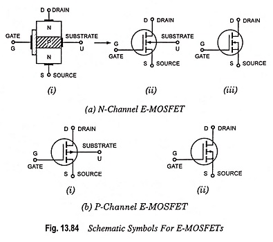
Schematic symbols for an N-channel E-MOSFET are shown in Fig. 13.84(a). For zero value of VGS, the E-MOSFET is OFF because there is no conducting channel between source and drain. Each of schematic symbols shown in Figs. 13.84(a) (ii) and 13.84(a) (iii), has broken channel line to indicate this normally OFF condition. As we know that for VGS exceeding the threshold voltage VGST, an N-type inversion layer, connecting the source to drain, is created. In each of the schematic symbols, the arrow points to this inversion layer, which acts like an N-channel when the device is conducting. In each case, the fact that the device has an insulated gate is indicated by the gate not making direct contact with the channel. The schematic symbol shown in Fig. 13.84(a) (iii) shows the source and substrate internally connected, while the other symbol shown in Fig. 13.84(a) (ii) shows the substrate connection brought out separately from the source.
The schematic symbols for a P-channel E-MOSFET are shown in Fig. 13.84(b). In these cases the arrow points outwards.
E-MOSFET Data Sheets:
As already mentioned above, there are three key quantities [ID (ON), VGST and VGS (ON)] with E-MOSFETs. Data sheets may vary from one manufacturer to another one and one may contain some information’s somewhat different from those given in another manufacturer’s data sheet. But almost all data sheets include information regarding VGST, ID (ON) and most include information regarding VGS (ON). Some also include information on the drain resistance RDS. This resistance may be symbolized RDS or it may appear as rDS (ON), rds (ON) etc.
MOSFET Biasing:
MOSFET bias circuits are quite similar to the circuits used for JPET biasing. In the case of DE-MOSFETs, the gate-source voltage VGS may be either positive or negative in both N-channel and P-channel devices. Any of the JFET bias circuits already discussed can be used to give a negative VGS for an N-channel device, or a positive VGS for a P-channel device. To operate an N-channel MOSFET in enhancement mode (either a DE-MOSFET or E-MOSFET), the gate is required to be biased positively with respect to the source. The self-bias circuit is unsuitable in such a case, and if fixed voltage bias is to be used, VGS must be a positive quantity. The same remarks apply for a P-channel MOSFET operating in E-mode, except that the gate must be made negative w.r.t. the source.
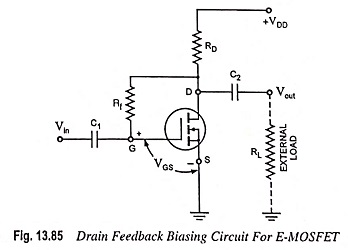
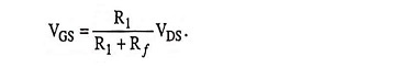
A popular circuit arrangement for biasing the N-channel E-MOSFET is shown in Fig. 13.85. Resistor Rf brings a suitably large voltage (VGS > VGST) to the gate to drive the E-MOSFET on. The drain current ID increases until an equilibrium condition of VDS (or VGS) and drain current ID is established. The MOSFET drain current is fixed by VGS as given by Eq. (13.62). The drain current ID causes a voltage drop across RD, so that
![]()
Since the gate current lG = 0, the voltage VGS = VDS, so Eq. (13.62) may be written as
![]()
With VS = 0 volt, the value of VDS is
![]()
If ID tries to increase due to some reason (say due to increase in temperature), VDS will decrease due to larger voltage drop in RD and cause VGS to decrease. So ID will decrease to overcome the original increase in ID. Thus operating or quiescent point remains fixed.
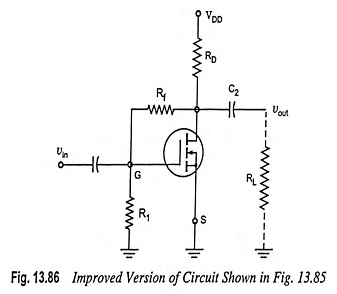
If for reasons of linearity in device operation or maximum output voltage, equality of VGS and VDS is not desirable, then the circuit shown in Fig. 13.86, known as drain-to-gate bias circuit may be used.
Here, the gate bias voltage is
This circuit also, like that shown in Fig. 13.85, offers the dc stabilization through the feedback resistor Rf However, the input resistance is reduced because of the Miller effect, Rf corresponds to an equivalent resistance, Rin = Rf(1 – AV) shunting the amplifier input.
Also, the voltage divider biasing technique (circuit shown in Fig. 13.87) can be used for E-MOSFET. Here the dc stability is accomplished by the feedback through source resistance RS.
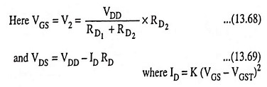
The value of resistors used in this divider circuit is quite high as E-MOSFET gate draws very little current due to the insulation layer.
E-MOSFET Amplifier:
An N-channel E-MOSFET having a potential divider bias is shown in Fig. 13.87. AC signal source is applied to the gate through coupling capacitor C1 and the gate is biased with a positive voltage such that VGS > VGST.
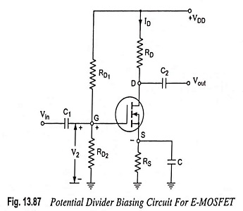
As illustrated in Fig. 13.88, the input signal voltage produces a swing below and above its Q-point. This, in turn, causes a swing in drain current ID. Thus VD or Vout varies being equal to VDD – IDRD.
E-MOSFET Equivalent Circuit:
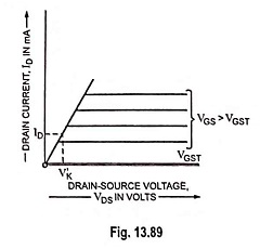
Ideal drain curves for an Enhancement Type MOSFET are shown in Fig. 13.89. All drain curves superimpose in the ohmic region to give a single, almost vertical line and are horizontal in the current-source region. There is no breakdown region. These ideal drain curves are similar to depletion-mode curves, except for the proportional knee voltage V′K, which is given as
![]()
This voltage V′K, is the border between the ohmic region and the current source region in an ideal enhancement-mode device. This border concept is identical to VP. Since E-MOSFET does not have a pinch-off voltage where depletion layers meet together, V′P is not used. Instead, they have an inversion layer. Because a different physical mechanism is involved, symbol V′K is used for the border between the two regions.
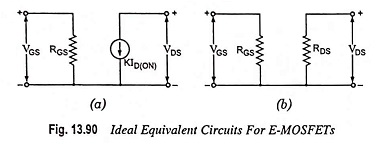
Two ideal equivalent circuits for an Enhancement Type MOSFET are shown in Fig. 13.90. These equivalent circuits are the same as for a JFET, except for ID (ON) and the positive gate-source voltage. In other words, the E-MOSFET can operate like a voltage variable resistor (VVR) or like a constant current source depending upon the location of the operating point. The proportional knee voltage is the guide. When VDS exceeds V′K, the device is a constant current device and VD below V’K, the device is a resistor.