Power BJT – Construction, Operation and its Characteristics:
Power transistors are large-area devices. Because of differences in geometry and doping concentrations, their properties tend to vary from those of the small-signal devices. The structure of a vertical NPN power transistor is shown in Fig. 26.74. In the vertical configuration for power BJT, the collector terminal is at the bottom of the device. This configuration is preferred as it maximizes the cross-sectional area through which the current flows in the device. In addition, the doping concentrations and dimensions are different from those of small switching transistors.
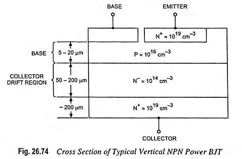
The primary collector region has a low-doped impurity concentration so that a large base-collector voltage can be applied without initiating breakdown. Another N region, with a higher doping concentration, reduces collector resistance and makes contact with the external collector terminal. The base region is also much wider than normally encountered in small devices. A large base-collector voltage implies a relatively large space-charge width being induced in both the collector and base regions. A relatively large base width is required to avoid punch-through breakdown.
Power transistors must also be large-area devices in order to handle large currents.
Power Transistor Characteristics:
The relatively wide basewidth implies a much smaller current gain β for power transistors in comparison to that of small switching transistors, and large area device implies a large junction capacitance and hence a lower cutoff frequency for a power transistor compared to a small switching transistor.
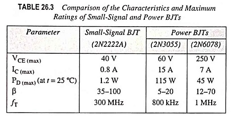
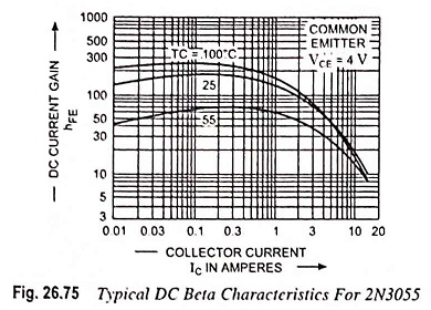
Table 26.3 compares the parameters of a general-purpose small signal BJT to those of two power BJTs. The current gain is generally smaller in power transistors, typically in the range of 20 to 100, and may be a strong function of collector current IC and temperature. Typical current gain-collector current characteristics for the 2N3055 power BJT at various temperatures are shown in Fig. 26.75.
The maximum rated collector current lCmax may be related to the maximum current that the wires connecting the semiconductor to the external terminals can handle, the collector current at which the current gain falls below a minimum specified value, or the current that leads to the maximum power dissipation when the transistor is biased in saturation.
The maximum rated voltage in a BJT is generally associated with avalanche breakdown in the reverse-biased base-collector junction. In the CE configuration, the breakdown voltage mechanism also involves the transistor gain, as well as the breakdown phenomenon in the PN junction. Typical lC versus VCE characteristics are depicted in Fig. 26.76. When the transistor is biased to operate in the forward active mode, IC begins to increase significantly before the actual breakdown voltage is reached. All the curves tend to merge to the same collector-emitter voltage VCE once breakdown has occurred. This voltage VCE sus is the minimum voltage necessary to sustain the transistor in breakdown.
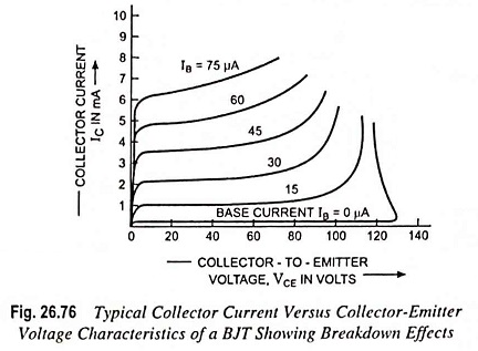
Another breakdown effect is known as second breakdown, which occurs in a BJT operating at high voltage and large current. Slight non-uniformities in current density develop local regions of increased heating that reduces the resistance of the semiconductor material, which in turn enhances the current in those regions. This effect results in positive feedback, and the current continues to rise, causing a further increase in temperature, until the semiconductor material may actually melt, creating a short-circuit between the collector and emitter and causing a permanent failure.
The instantaneous power dissipation in a BJT is given as
![]()
The base current is generally much smaller than the collector current; therefore, to a good approximation, the instantaneous power dissipation is
![]()
The average power, which is determined by integrating above Eq. (26.27) over one cycle of the signal, is
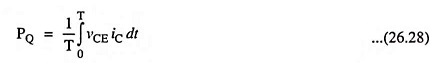
The average power dissipated in a BJT must be kept below a specified maximum value, to ensure that the temperature of the device remains below a maximum value. If lC and VCE are assumed to be dc quantities, then at the maximum rated power PT for the transistor, we may write
![]()
The maximum current, voltage and power limitations can be illustrated on the lC versus VCE characteristics as depicted in Fig. 26.77. The average power limitation PT is a hyperbola described by Eq. (26.29). The region where the transistor can be operated safely is known as the safe operating area (SOA) and is bounded by IC max, VCE sus, PT and the transistors second breakdown characteristic curve.
The iC – vCE operating point may move momentarily outside the SOA without damaging the transistor, but this depends on how far the Q-point moves outside the area and for how long. For our purposes, it is assumed that the device must remain within the SOA at all times.
Darlington Pair Configuration:
As mentioned, the basewidth of a power BJT is relatively wide so that the current gain is relatively small. Higher current gain can be had if we make use of a Darlington pair, as shown in Fig. 26.78. The pair can be fabricated on one chip, or two discrete transistors can be physically connected to form a Darlington pair. The emitter current of the first transistor drives the second transistor. Therefore, the overall current gain increases.
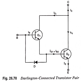
Considering the currents, we see that
![]()
The overall common-emitter current gain is then
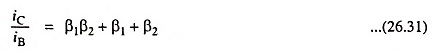
Thus, if the gain of each individual transistor is β1 = β2 =20, then the overall current gain of the Darlington pair is iC/iB = 440. This overall current gain is significantly larger than that of the individual device. A diode may be incorporated, as shown in Fig. 26.78 to assist in turning off the transistor Q2. A reverse current out of the base of transistor Q2 through the diode will pull charge out of the base of this transistor and turn the device off faster than when no diode is used.
The Darlington pair shown in Fig. 26.78 is typically employed in the output stage of a power amplifier when an NPN transistor is required. A PNP Darlington pair may also be used to enhance the effective current gain of a power PNP device.
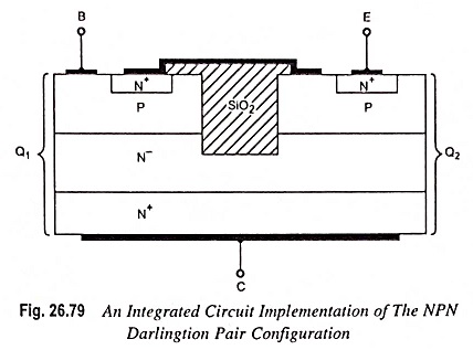
The integrated circuit configuration of the NPN Darlington pair may be as illustrated in Fig. 26.79. The SiO2 that is shown completely penetrates through the P-type base region so that the base regions of the two transistors are isolated.