Emitter Follower Circuit – Operation, Advantages and Applications:
Emitter Follower Circuit is also a negative current feedback circuit. This circuits exhibits a large input impedance, a small output impedance, and a voltage gain of approximately unity. Further the output voltage tends to be in phase with the input voltage—hence the term “follower”.
At first glance, one might be tempted to dismiss such a circuit as useless because of its unity voltage gain. However, its input and output impedances promote its use as input and output buffer stages in amplifier systems.
The circuit of an emitter follower circuit is shown in Fig. 19.43. The main difference between an emitter follower and conventional amplifier is the absence of collector load and emitter bypass capacitor. The emitter resistance RE itself acts as the load and the ac output voltage Vout is taken across it. The biasing is provided either by base resistor method or potential divider method.
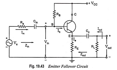
The circuit consists of a resistance of the order of 10 kΩ in the emitter itself and the collector is connected directly to the supply. Stabilization of operating point is exceptionally good because of high value of emitter resistance RE.
Operation of Emitter Follower Circuit:
When input signal Vs is applied to the base, the resulting emitter current Ie develops an output voltage Vout equal to IeRE across the emitter resistance RE. This voltage opposes the ac signal voltage Vs as it is in phase opposition to Vs. Thus it provides negative current feedback. Moreover, this voltage (Vout) fed back to the input is proportional to the emitter current hence this circuit is called a negative current feedback circuit.
It may be noted that when the input signal voltage Vs goes through its positive half cycle the output voltage Vout is also seen to go through its positive half cycle. Hence the output voltage is in phase with the input signal voltage i.e., the output voltage (emitter voltage) just follows the input voltage and hence the name emitter follower.
Circuit Analysis:
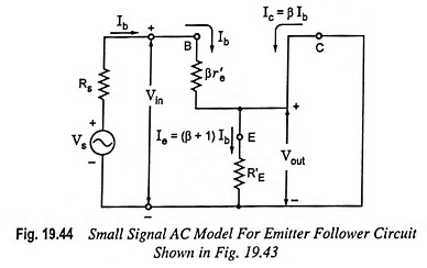
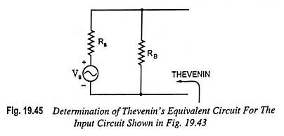
For the emitter follower configuration given in Fig. 19.43, the small-signal ac model is drawn, as illustrated in Fig. 19.44. For the input section of Fig. 19.44, the resistance RB is neglected because it is usually much larger than source resistance Rs that a Thevenin’s equivalent circuit for the configuration of Fig. 19.45 would result in simply Rs and Vs as illustrated in Fig. 19.44. Of course, if current levels are to be determined such as Iin in the original diagram, the effect of RB is to be considered.
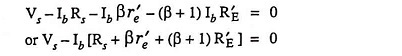
Applying Kirchhoff’s voltage law to the input circuit of Fig. 19.44, we have
Emitter current,
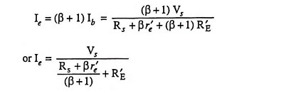
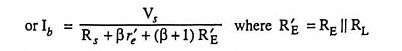
Taking (β + 1) ≡ β, we have
Emitter current,
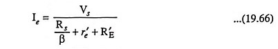
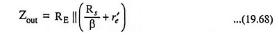
Now a network is drawn following the above equation and is given in Fig. 19.46 (a). In Fig. 19.46 (b) RE and load resistance RL have been segregated to define output impedance Zout and output current lout.
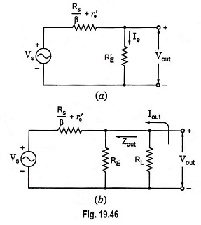
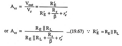
The voltage gain can then be had directly from Fig. 19.46 (a) using the voltage divider rule
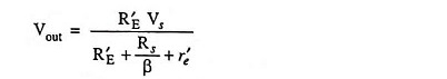
and voltage gain,
Setting Vs = 0 and solving for Zout we have
For the input impedance,
![]()
and input impedance
![]()
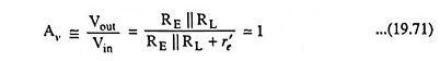
For no-load conditions the gain equation becomes
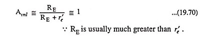
while for loaded condition
Current gain,
![]()
From circuit shown in Fig. 19.43, input voltage to the amplifier, which equals Vbe, is given as
![]()
neglecting voltage drop in source resistance Rs.
So the feedback ratio β i.e., feedback is 100%.
Advantages:
- High input impedance and low output impedance, so it can be used for impedance matching. Sometimes it is called impedance transformer.
- Because of 100 per cent feedback, output is distortion less and bandwidth is very large.
- Relatively high current gain and power gain.
- Output and input ac voltages are in phase and also approximately equal in magnitude i.e., emitter output voltage closely follows the input and so it is called the emitter follower.
Applications:
Because of high input impedance and low output impedance an emitter follower circuit is capable of transferring maximum power from the high impedance source to low impedance load. When an emitter follower is employed for this purpose, it is called a buffer amplifier. Though impedance matching can be achieved by employing a step-down transformer but emitter follower is preferred. It is because emitter follower circuit is not only more convenient than a transformer but it also provides better frequency response.
There are many instances (especially in digital electronics) where an increase in current is required but no increase in voltage is required. For such situations emitter follower, because of its high current gain, can be employed.