Transistor approximation (Ideal, Second and Higher):
An NPN transistor is shown in Fig. 10.71 (a). Voltage appearing across the emitter diode is denoted by VBE and that appearing across the collector-emitter terminals is denoted by VCE.
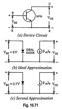
Ideal Approximation: An ideal approximation of a transistor is shown in Fig. 10.71 (b). Emitter diode is visualized as an ideal diode. In this case, VBE = 0. This makes calculation of base current quick and easy. This equivalent circuit is often useful for troubleshooting when approximate value of IB is needed.
The collector side of the transistor acts as a current source that pumps a collector current of βdcIB through the collector resistor. Thus collector current can be obtained simply by multiplying base current IB by current gain.
Second Approximation: Second approximation of a transistor is depicted in Fig. 10.71(c). This is more commonly used because it may improve the analysis significantly when the base supply voltage is small. Base current is usually determined by using second approximation of the diode. Here VBE is taken equal to 0.7 V in case of silicon transistors and 0.3 V in case of germanium transistors. With the second transistor approximation, the base and collector currents will be slightly less than their ideal values.
Higher Approximations: The bulk resistance of the emitter diode becomes significant only in high power applications in which the currents are large. The effect of bulk resistance in the emitter diode is to increase VBE to more than 0.7 V. For instance, in some high power circuits, the VBE across the base-emitter diode may exceed 1 V.
Likewise, the bulk resistance of the collector diode may have a noticeable effect in some designs. Besides emitter and collector bulk resistances, a transistor has many other higher order effects that make hand calculations tedious and time consuming. For this reason, calculations beyond the second transistor approximation should use a computer solution.