Transistor Action : Operation of PNP Transistor:
Transistor action – Transistors of both types (P-N-P and N-P-N) behave exactly in the same way except change in biasing and majority carriers. In P-N-P transistors the conduction is by holes whereas in N-P-N transistors conduction is by electrons. However, N-P-N transistors are preferred due to their better high frequency response.
Unbiased Transistor:
When no battery is connected between the different terminals of a transistor, the transistor is said to be in an unbiased state or in an open-circuit state.
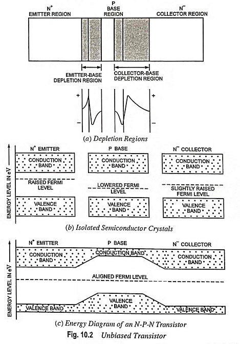
We know that when a semiconductor is doped with donor or pentavalent impurities, it becomes an N-type semiconductor. The additional free electrons tend to raise the Fermi (average electron energy) level within the crystal. Similarly, when a semiconductor is doped with acceptor or trivalent impurities, it becomes a P-type semiconductor. The additional holes tend to lower the Fermi level. This transistor action is illustrated in Fig. 10.2 (b).
We also know that when an N-type region is formed next to a P-type region, a barrier potential (0.7 V in case of Si and 0.3 V in case of Ge at room temperature) is produced at the P-N junction. The free electrons in the N-region diffuse into the adjacent P-region to annihilate holes. Consequently, a layer of positive ions is formed on the N side, and a layer of negative ions is formed on the P-side. This serves to create the barrier potential.
The same phenomenon occurs at both the P-N junctions found in the N-P-N transistor structure [Fig. 10.2(a)]. The depletion regions (ionization layers), which are formed, extend into the semiconductor crystal as a function of the doping levels. Specifically, it extends deeply into the lightly doped regions, and slightly into the heavily doped regions. Since emitter is heavily doped than base and collector, the emitter-base depletion region width is smaller than that of collector-base depletion region width. Note that the barrier potentials are negative on the base and positive on the emitter and collector for the N-P-N device. In case of P-N-P device it would be just reverse i.e., positive on the base and negative on emitter and collector. This transistor action is illustrated in Fig. 10.2(a).
The formation of barrier potential corresponds to the alignment of the Fermi levels throughout the crystals. Fermi level alignment produces a distortion in the valence and conduction energy bands, as illustrated in Figs. 10.2(b) and 10.2(c).
Operation of Transistor:
The process of applying dc voltages across the different terminals of a transistor is called biasing. For normal operation the emitter-base junction is always forward biased while the collector-base junction is always reverse biased. This transistor action is depicted in Fig. 10.3.
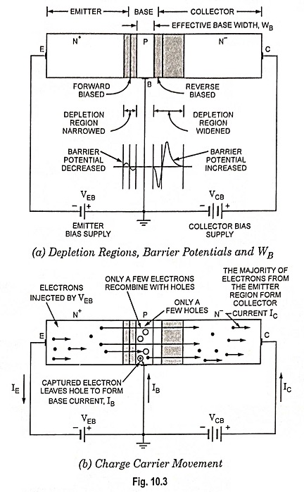
The forward bias at the emitter-base junction reduces the barrier potential and narrows the depletion region. However, the relatively lightly doped base and collector regions produce a wide depletion region under the reverse bias. The noteworthy point is that the effective base width Wb between the two depletion regions is very narrow. This transistor action is illustrated in Fig. 10.3(a).
Electrons are injected into the emitter region by the emitter bias supply VEB. These conduction band electrons have enough energy to overcome the emitter-base barrier potential. The injected electrons enter the very thin, lightly doped base region (electrons are minority carriers in the P-type base region). Because the base is very lightly doped relative to the emitter region, only a few of the electrons recombine with the holes doped into the base.
Injection of electrons makes the electrons concentration on the emitter junction very large and on the collector junction the concentration of the electrons is extremely small and as such the gradient of electron concentration is very large in base. Injected electrons diffuse into collector region due to extremely small thickness of base which is much less than the diffusion length. Most of the electrons cross into the collector region. Collector is reverse biased and creates a strong electrostatic field between base and collector. The field immediately collects the diffused electrons which enter the collector junction. Flow of electrons into the base region when confronted with the holes, a few electrons (say 1 to 5%) combine and neutralize and rest of the electrons (say 95 to 99%) of the injected electrons diffuse into the collector region and collected by the collector electrode. For each electron that combines with a hole, an electron leaves the base region via the base terminal. This transistor action creates a very small base current (1 to 5% of the electron current from emitter to collector). Thus the emitter current IE is equal to the sum of collector current lC and base current lB. The ratio of collector current lC to emitter current Ie is called the α and it is measure of the possible current amplification. In a transistor α cannot be higher than unity, but practical values of 0.95 to 0.99 are attained in commercial transistors.
The operation of the transistor may also be examined by means of its energy band diagram. Since the forward bias tends to align the valence and conduction energy bands, while reverse bias tends to increase their misalignment, the diagram shown in Fig. 10.4 is arrived at. As can be seen from Fig. 10.4, electrons must lose energy to travel from the emitter region to the base region. Further, the electrons must also lose energy in moving from base region into collector region. Only a few of the electrons in the base region lose energy to recombine with the (valence band) hole. Typically, at least 95% of the electrons have a long enough lifetime to diffuse into the collector region.
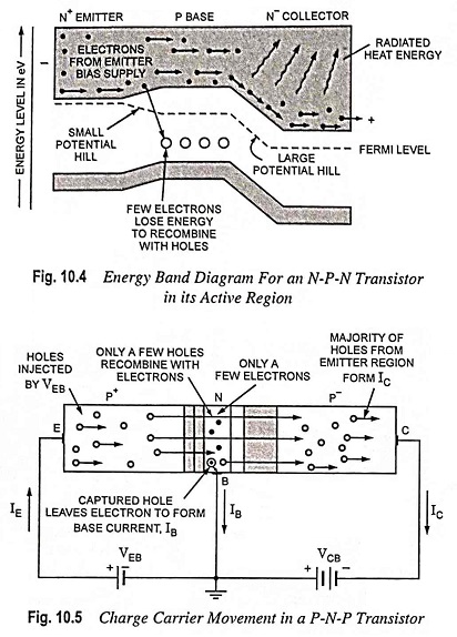
It is observed from Fig. 10.4 that the potential hill (bend in the Fermi level) between the base and the collector region is very steep. Specifically, the electrons must lose a considerable amount of energy as they move from the base region to the collector region. Typically, the electrons give up their energy in the form of heat. Consequently, the collector region must be able to dissipate this heat energy. It is for this reason that it is typically the largest of the three regions.
Operation of P-N-P Transistor:
The P-N-P transistor behaves exactly the same way as an N-P-N device, with the exception that the majority charge carriers are holes. As illustrated in Fig. 10.5, holes are emitted from the P-type emitter across the forward-biased emitter-base junction into the base. In the lightly doped N-type base, the holes find few electrons to recombine with. Some of the holes flow out via the base terminal, but most are drawn across the collector by the positive-negative electric field at the reverse biased collector-base junction. As in the case of NPN device, the forward bias at the emitter base junction controls the collector and emitter currents.