Diode as a Circuit Element:
Diode as a Circuit Element – The P-N junction diode is considered as a circuit element. One of the most important application of diode is in rectification (i.e., in conversion of sinusoidal ac supply into dc supply).
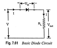
The basic diode circuit, shown in Fig. 7.61, consists of a diode in series with a load resistance RL across an input voltage of V volts.
Load Line Concept
Kirchhoff s voltage law is applicable both to linear and nonlinear circuits, so we may write
![]()
where I is the circuit current.
![]()
The above equation provides a linear relation between the diode or circuit current I and the diode voltage VD for a given input voltage V and load resistance RL. This equation is referred to as the circuit load line, and is usually plotted on graph with the current I as the vertical axis and the voltage VD as the horizontal axis. From Eq. (7.40), we see that for current I = 0, VD = V which is the horizontal axis intercept. Also from this equation, if VD = 0, then current I = V/RL which is the vertical axis intercept. The load line can be drawn between these two points. The slope of the load line is determined by RL, the negative value of the slope is equal to 1/RL.
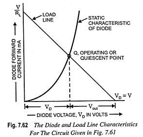
The intersection of load line with the static characteristic of diode provides the operating point, sometimes referred to as quiescent or Q point. The dc load line illustrates all dc conditions that could exist within the circuit for given supply voltage V and load resistance RL.
The graphical analysis method can yield accurate results, but it is somewhat cumbersome. However, the concept of load line and the graphical approach are useful for “visualizing” the response of the circuit and the load line is used extensively in the evaluation of electronic circuits.
Dynamic Characteristics. Now let a variable voltage vin be applied to a diode circuit, depicted in Fig. 7.63. A plot of current i vs input voltage vin is called the dynamic characteristic. The curve is drawn for different values of input voltage vin.
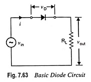
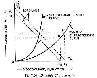
Figure 7.64 depicts the load lines for two voltages vin and v′in. It is observed from Fig. 7.64 that the load lines drawn for the two input voltages vin and v’in are parallel to each other. This is because slope of the load line does not vary with the change in input voltage since RL is constant. The load lines intersect the static characteristics at points A and A’ respectively. Now, vertical lines are drawn from vin and v’in and horizontal lines are drawn from points A and A’ respectively. A curve drawn passing through B’BO is known as dynamic characteristic.
Transfer Characteristic. The curve that relates the output voltage vout to the input voltage vin of any circuit is known as the transfer or transmission characteristic. Figure 7.65 illustrates the graphical method for determination of output voltage waveform for a given input voltage waveform (say, sinusoidal waveform) using transfer characteristic.
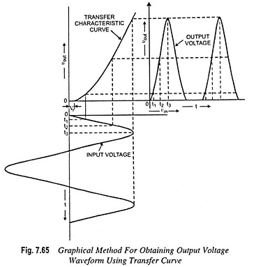
The input signal waveform is drawn with its time axis vertically downward, so that the voltage axis is horizontal. The different input voltages are at different time instants t1, t2, t3 etc. and corresponding vertical lines are drawn to meet the transfer curve. Now horizontal lines are drawn from the intersection points on transfer curve to provide the output voltage corresponding to time instants t1, t2, t3 etc. Thus output voltage waveform can be obtained by joining these points. From Fig. 7.65, it can be visualized that (i) the output voltage is distorted at the start due to nonlinear transfer characteristic and (ii) for vin < Vr, the diode acts as a clipper and a portion of the input signal does not appear at the output.