Diode Clamping Circuit – Positive and Negative Clamping:
Diode Clamping Circuit – A circuit that places either the +ve or -ve peak of a signal at a desired level is known as a clamping circuit. It simply adds or subtracts a dc component to the input signal. In steady state, the output waveform is an exact replica of the input waveform. The clamper is also referred to as a dc restorer and a (signal) level shifter.
The necessity to establish the extremity of the positive or negative signal excursion at some reference level (i.e., to introduce a dc component to the input signal) arises in connection with a signal that has passed through a capacitive coupling network and lost its dc component, as in case of television receivers. However, normally the dc component introduced is not identical with the dc component lost in transmission.
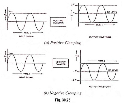
In fact, a clamp circuit adds dc component (positive or negative) to the input signal so as to push it either on the positive side, as illustrated in Fig. 30.75 (a) or on the negative side, as illustrated in Fig. 30.75 (b). When the circuit pushes the signal on the positive side or upward, the negative peak of the signal coincides with the zero level and the circuit is called the positive damper. On the other hand, when the signal is pushed on the negative side or downward, as illustrated in Fig. 30.75 (b), the positive peak of the input signal coincides with the zero level and the circuit is called the negative damper.
For a clamping circuit at least three components—a diode, a capacitor and a resistor are required. Sometimes an independent dc supply is also required to cause an additional shift.
The important points regarding diode clamping circuits are:
- Waveform remains the same but its level is shifted either upward or downward.
- The clamping circuit does not change the peak-to-peak or rms value of the waveform. Thus referring to Fig. 30.75, the input waveform and output waveform have the same peak-to-peak value i.e., 2 Vmax. If the input voltage and clamped output are measured by an ac voltmeter, the readings will be the same.
- The clamping circuit, of course, alters the peak and average values of the waveform. In Fig. 30.75 the input waveform has a peak value of Vmax and average value over a complete cycle is zero. The clamped output varies from 2 Vmax and 0 (or 0 and – 2 Vmax). Thus the peak value of the clamped output is 2 Vmax and average value is Vmax.
- Both resistors R and C affect the waveform.
- The values of R and C should be taken such that the time constant of the circuit τ = RC is large enough to ensure that the voltage across the capacitor C does not change significantly during the interval the diode is non-conducting. For good clamping action, the circuit time constant τ = RC should be at least ten times the time period of the input signal voltage.
It is advantageous to first consider the condition under which the diode becomes forward biased.
Diode Clamping circuits are often employed in television receivers as dc restorers. The incoming composite video signal is normally processed through capacitively coupled amplifiers which eliminate the dc component thereby losing the black and white reference levels and the blanking level. These reference levels have to be restored before applying the video signal to the picture tube. This is accomplished by employing clamping circuits. Diode Clamping circuits are also used in storage counter, analog frequency meter, capacitance meter, divider and staircase waveform generator.
Consider a negative clamping circuit, a circuit that shifts the original signal in a vertical downward direction, shown in Fig. 30.76. With the positive input, the diode D is forward biased and capacitor C is charged with the polarity shown. During the positive half cycle of input, the output voltage is equal to barrier potential of the diode, V0 and the capacitor is charged to (V – V0). When the input goes negative, the diode is reverse biased and acts as an open circuit and thus has no effect on the capacitor voltage. R being of very high value cannot discharge C by very much during the -ve portion of the input waveform. Thus during negative input, the output voltage being the sum of the input voltage and the capacitor voltage is equal to – V – (V – V0) or – (2 V – V0). Thus peak-to-peak output being the difference of the negative and positive peak voltage levels is equal to V0 – [- (2 V – V0)] or 2 V.
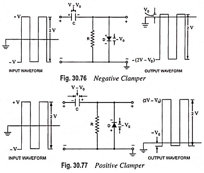
If the diode in Fig. 30.76 is reconnected with reversed polarity, the circuit becomes a positive clamping circuit. The positive clamping circuit shifts the original signal in a vertical upward direction. A positive clamping circuit is shown in Fig. 30.77. It contains a diode D and a capacitor C as are contained in a negative clamper. The only difference in the circuit is that the polarity of the diode is reversed. Because of this reason the circuit acts as a positive clamper. The remaining explanation regarding the working of the circuit is the same as is explained for the negative clamper.
To remember which way the dc level of a signal moves, look at Fig. 30.76. Notice that the diode arrow points downward, the same direction as the dc shift. Similarly in Fig. 30.77, the diode arrow points upward, again the same direction as the dc shifts. It means that, when the diode points upward, we have a positive dc clamper and when the diode points downward, the circuit is a negative dc clamper.
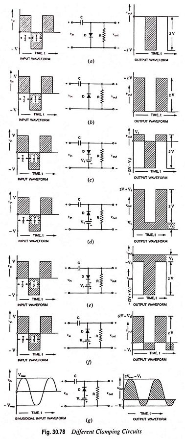
A number of clamping circuits with their effect on the input signal are shown in Fig. 30.78. Although all the waveforms appearing in Fig. 30.78 are square waves, clamping networks operate equally well for sinusoidal inputs. In fact, one approach to the analysis of clamping networks with sinusoidal inputs is to replace the sinusoidal wave signal by a square wave of the same peak values. The resulting output will then form an envelope for the sinusoidal response, as illustrated in Fig. 30.78 (g) for a network appearing in Fig. 30.78 (f). The diodes have been assumed to be ideal and 5 RC >> T/2 in drawing the output waveforms.