What is Transistor Biasing? – Types of Biasing
As already mentioned, for normal operation of a transistor emitter-base junction is always forward biased and collector-base junction is always reverse biased. For a moment if the Transistor Biasing of emitter-base junction is ignored and only collector-base junction, which is reverse biased [Fig. 10.6 (a)] is considered, then due to high resistance of reverse biased collector diode, practically no current would flow in the collector circuit.
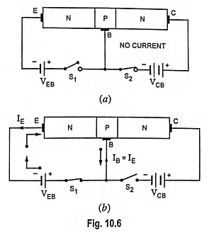
Now if the Transistor Biasing of collector-base junction is ignored and only emitter-base junction, which is forward biased [Fig. 10.6(b)] is considered then practically whole of the emitter current flows through the base i.e., IB = IE.
However, if the emitter-base junction is forward biased and the collector-base junction is reverse biased it is seen that almost whole (about 95%) of the current constituted by the emitter flows through collector circuit. Thus the magnitude of collector current lC depends upon the magnitude of emitter current IE. No emitter current means almost no collector current. This is precisely what happens in a transistor.
Different Operating Conditions For a Transistor:
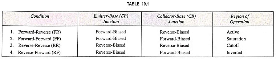
A transistor has two junctions (emitter-base and collector-base junctions), and each of these two junctions, may be forward biased or reverse biased, therefore, there are four possible ways of Transistor Biasing these two junctions. Accordingly it may operate in different conditions as listed in Table 10.1.
1. Forward-Reverse Biasing: As already mentioned, for normal operation of a transistor emitter-base junction is always forward biased and collector-base junction is always reverse biased. This type of Transistor Biasing is known as FR biasing. For this purpose a battery VEB is connected between emitter and base while a battery VCB is connected between the collector and base, as shown in Fig. 10.7. In Fig. 10.7(a), the emitter-base junction of N-P-N transistor is forward biased by connecting the negative terminal of battery VEB to the emitter and positive terminal to the base while collector-base junction is reverse biased by connecting the positive terminal of the battery VCB to the collector and negative terminal to the base. Similarly in Fig. 10.7(b) the emitter-base junction of P-N-P transistor is forward biased by connecting the positive terminal of battery VEB to the emitter and negative terminal to the base while collector-base junction is reverse biased by connecting the negative terminal of battery VCB to the collector and positive terminal to the base.
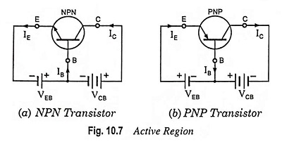
Typical base-to-emitter voltages for both N-P-N and P-N-P transistors are 0.7 V for silicon and 0.3 V for germanium. Typical collector-to-base voltages might be anything between 3 V and 20 V for most types of transistors, although in many cases the collector-to-base voltage may exceed 20 volts even.
The voltages across the terminals of a transistor follow the usual double subscript voltage convention. For example VBE represents the voltage of base with respect to the emitter. If VBE is equal to 0.7 V it means the base is 0.7 V more positive.
In FR biasing the transistor is in active region and the collector current IC, depends upon the emitter current IE. Generally transistor is operated in this region for amplification.
For connecting batteries properly in the transistor circuits the following scheme may be remembered.
The battery polarities to the emitter and base are the same as the letter of the emitter and base impurity designations. Thus, in the P-N-P type, the emitter receives the P (positive) terminal, and the base receives the N (negative) terminal. Similarly, in N-P-N type, the emitter receives the N (negative) terminal, the base receives the P (positive) terminal. The collector receives a battery polarity opposite to its impurity type designation. Thus P-type collector receives the N (negative) terminal of the battery and the N-type collector receives the P (positive) terminal.
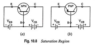
2. Forward-Forward Biasing: In this Transistor Biasing, both collector and emitter are forward biased, as illustrated in Fig. 10.8. The transistor operates in saturation region. In this region, the collector current becomes independent of the base current. Thus the transistor acts like a close switch.
3. Reverse-Reverse Biasing: In this Transistor Biasing, both the junctions are reverse biased. In this biasing, the transistor has practically zero current because the emitter does not emit charge carriers into the base and no charge carriers are collected by the collector except a few thermally generated minority carriers. Thus, the transistor acts like an open switch.
4. Reverse-Forward Biasing: In this Transistor Biasing, the emitter junction is reverse biased while the collector junction is forward biased. As the collector is not doped to the extent as the emitter is doped, therefore, it cannot inject the majority charge carriers to the base. So, in this region, the action of transistor is poor. This region is of little importance.
The active mode which is also called forward active mode, is the one used if the transistor is to operate as an amplifier. Switching operations (e.g., logic circuits) utilize both the cutoff mode and the saturation mode. The reverse active (or inverse active) mode has very limited application but is conceptually significant.