MOSFET Biasing Circuits:
DE-MOSFET Bias Circuits – DE-MOSFET bias circuits are similar to JFET bias circuits. Any of the FET bias circuits already discussed can be used to produce a negative VGS level for an n-channel MOSFET Biasing Circuits, or a positive VGS for a p-channel device. In this case, both devices would be operating in the depletion mode, just like JFETs. To operate an n-channel DEMOSFET in the enhancement mode, the gate terminal must be made positive with respect to the source. A p-channel DE-MOSFET in the enhancement mode requires the gate to be negative with respect to the source.
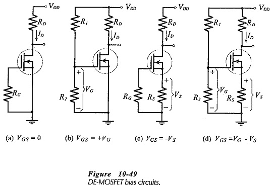
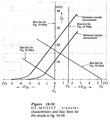
Consider the four MOSFET Biasing Circuits shown in Fig. 10-49, and assume that each device has the transfer characteristics in Fig. 10-50. In Fig. 10-49(a) the gate-source bias voltage is zero, so, the bias line is drawn on the transfer characteristics at VGS = 0, as shown in Fig 10-50. The FET in Fig. 10-49(b) has a positive gate-source bias voltage, consequently, its bias line must be drawn vertically at VGS = +VG. The self bias circuit in Fig. 10-49(c) has its bias line drawn from ID = 0 and VGS = 0 at a slope determined by RS, exactly as for a JFET self bias circuit. Similarly, the bias line for the voltage divider bias circuit in Fig. 10-49(d) is drawn from the point where ID = 0 and VGS = + VG with a slope set by RS.
As always, ID(min) and ID(max) for any circuit are indicated by the bias line intersections with the maximum and minimum transfer characteristics. Fig. 10-50 shows that in some cases the FET is operating in depletion mode, and in other cases it is operating in enhancement mode. Analysis and design procedures for these circuits are essentially the same as for similar JFET bias circuits.
MOSFET Biasing Circuits can also be used with a plus/minus supply voltage, as discussed already.
E-MOSFET Bias Circuits:
Enhancement MOSFETs (such as the VMOS and TMOS devices) must have positive gate-source bias voltages in the case of n-channel devices, and negative VGS levels for a p-channel FET. Thus, the gate bias circuit in Fig. 10-49(b) and the voltage divider bias circuit in Fig. 10-49(d) are suitable. In each case, the bias line is drawn exactly as already discussed.
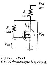
The drain-to-gate bias circuit shown in Fig. 10-53 is uniquely suitable for an E-MOSFET. The FET gate is directly connected to the drain terminal via resistor RG, so that VGS = VDS. Also,
![]()
If the drain current is higher than the design level, a higher voltage drop is produced across RD, and this tends to reduce VGS, and thus reduce ID back toward the design level. Similarly, a lower than intended ID level produces a lower IDRD voltage drop, and results in a higher VGS that drives ID back up toward the desired current. Corresponding levels of ID and VGS can be calculated from Eq. 10-19. These are then plotted on the device transfer characteristics to draw the circuit bias line.