Thermal Resistance – Definition, Circuit Diagram and Equation:
With power transistors, a designer often uses a heat sink to get a high power rating for the transistor. As already mentioned, the heat sink allows the internally generated heat to escape more easily from the transistor. This reduces the junction temperature, equivalent to increase the maximum power rating. To design a heat sink for a power transistor, we must first consider the concept of thermal resistance θ, which has the units of °C/W.
The heat developed at the collector-base junction of a transistor must flow from the junction to the transistor case, then from the case to the heat sink, and finally from heat sink to the surrounding air. Each portion of the path that the heat must pass through has a thermal resistance. These thermal resistances are θjC (junction to case), θCS (case to sink), and θSA (sink to air).
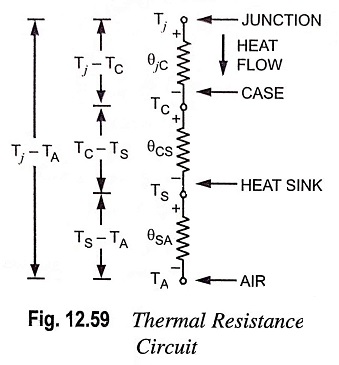
Thermal equivalent circuit for the transistor and heat sink is depicted in Fig. 12.59. This consists of the three thermal resistances connected in series. The size of heat sink required for a transistor with given power dissipation, PD may be determined from the thermal equivalent circuit. The temperature difference between the transistor collector-base junction and the air surrounding the heat sink (Tj – TA) causes the dissipated power (PD) to flow through each of the thermal resistances in series.
The thermal resistance series circuit is analogous to an electrical series resistive circuit—temperature difference is the electrical analog of voltage drop, and power or heat flow is the electrical analog of current. Ohm’s law may be applied to a thermal series circuit exactly as in the case of an electrical series circuit. So for a series thermal resistance circuit,
Power flow,

where temperatures are in degrees Celsius (°C), thermal resistances are in degrees Celsius per watt (°C/W) and PD is the power dissipated in watts.
Manufacturer’s data sheets for power devices generally provide the maximum operating junction or device temperature Tjmax and the thermal resistance from the junction to the case, θjC. Total thermal resistance between the junction and surroundings may be determined from the relation
As a guide, θCS is from 0.2 to 1°C per watt and θSA is from 1 to 100°C per watt depending on the size of the heat sink, number of fins, finish, and other factors.
Condition For Thermal Stability:
The condition required to avoid the thermal runaway is given below :
The rate at which heat is released at the collector junction must not exceed the rate at which the heat can be dissipated under steady-state condition
where PC is the heat released at collector and PD is the maximum power dissipated.
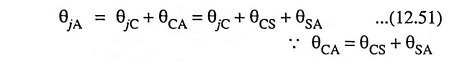
From Eqs. (12.50) and (12.51)
![]()
Differentiating above equation w.r.t. Tj, we have
Substituting ∂PD/∂Tj = 1/θjA in Eq. (12.52), we have
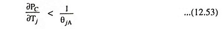
The condition expressed by Eq. (12.53) is the condition which must be satisfied to avoid thermal runaway. By suitable design, it is possible to ensure that the transistor cannot runaway before a specified ambient temperature or even under any condition.