Single Input Balanced Output Differential Amplifier:
In a single input balanced output differential amplifier an input signal is applied to either input, with the other input connected to ground. However, due to the common-emitter connection the input signal operates both transistors, resulting in output from both collectors.
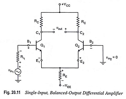
Single input balanced output differential amplifier is depicted in Fig. 20.11. In this circuit, an input signal is applied to the base of transistor Q1, with the other input connected to ground. Output is measured between the two collectors, which are at the same potential, and that is why the output is said to be balanced output.
DC Analysis:
The dc analysis process and the bias equations for this configuration are identical to those of the two previous configurations. This is because the dc equivalent circuit for all the three configurations is the same. Hence the quiescent collector current ICQ and quiescent collector-emitter voltage VCEQ are given by the expressions

AC Analysis:
Figure 20.12(a) depicts the ac equivalent circuit of this configuration with small signal T-equivalent models substituted for the transistors.
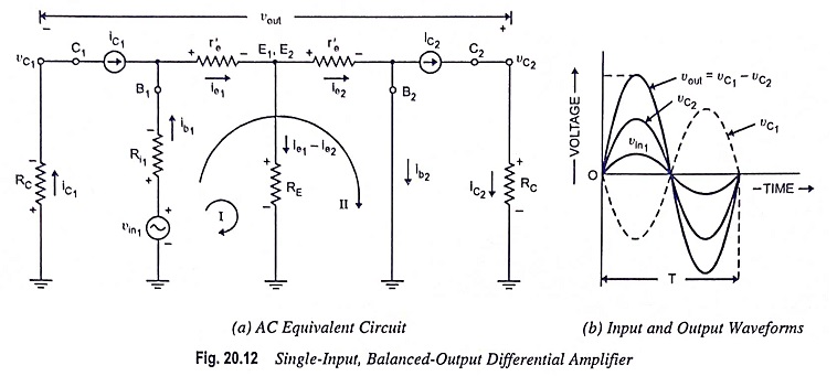
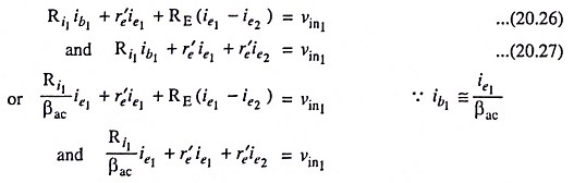
1. Voltage Gain: First of all let us discuss the important points about the circuit depicted in Fig. 20.12(a).
(i) During the positive half-cycle of the input signal vin1, the VBE for the transistor Q1 is positive and that of transistor Q2 is negative, as indicated in Fig. 20.11. Thus the collector current in transistor Q1 increases and that in transistor Q2 falls from the quiescent value ICQ. This change in collector currents during the positive half cycle of the input signal is shown in Fig. 20.12(a) by indicating them flowing in the same direction. During the negative half-cycle of input signal vin1, the the opposite action takes place i.e. iC1 falls and iC2 strengthens.
(ii) The voltage across the collector resistance of transistor Q2 is positive, and that across the transistor Q1 is negative with respect to ground. This is because the voltage across each resistor is consistent with the direction of current sources iC1 and iC2.
(iii) The output voltage vout is equal to the difference of voltages at the two collectors C1 and C2 i.e. vout = vC1 -vC2.
Applying KVL to loops I and II of the circuit given in Fig. 20.12 (a), we have
Usually Ri1/βac is negligibly small; therefore, neglecting it for simplicity, we have
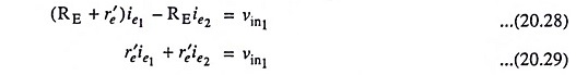
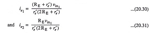
Solving above equations for ie1 and ie2, we have
The output voltage,
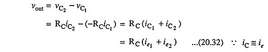
Substituting the values of ie1 and ie2 from Eqs. (20.30) and (20.31) respectively in Eq. (20.32), we have
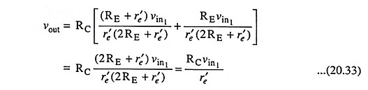
Thus voltage gain,
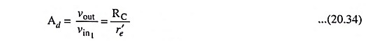
The above equation reveals that the voltage gain of the single input balanced output differential amplifier is equal to that of dual-input, balanced-output differential amplifier [Eq. (20.15)]

The input and output waveforms for this configuration are shown in Fig. 20.12 (b).
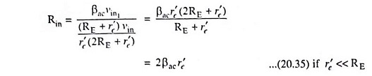
2. Differential Input Resistance: The input resistance Rin seen from the input signal source is given by expression
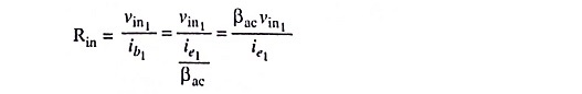
Substituting the value of ie1 from Eq. (20.30) in above equation, we have
3. Output Resistance: The output resistance measured at collector C1(Rout1) and the output resistance measured at the collector C2(Rout2) are given by equation
![]()