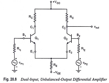
Dual Input Unbalanced Output Differential Amplifier:
It is an important configuration and converts dual inputs into a single ended output. In this configuration, two input signals are applied and the output is measured at only one of the two collectors (either at C1 or at C2) with respect to ground. The output is called the unbalanced output because the collector at which the output voltage is measured is at some finite dc potential w.r.t. ground. It means that there is some dc voltage at the output terminal even in the absence of any input signal.
Let the output be measured at the collector of transistor Q2 w.r.t. ground. This configuration is depicted in Fig. 20.8.
DC Analysis:
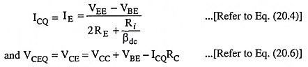
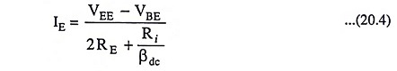
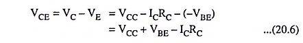
DC analysis for dual-input unbalanced-output differential amplifier is identical to that of the dual-input, balanced-output differential amplifier. This is because the biasing arrangement employed in both configurations is same. Hence the quiescent collector current ICQ and quiescent collector-emitter voltage VCEQ are given by equations
AC Analysis:
An ac equivalent circuit of the dual input unbalanced output differential amplifier, with small-signal T-equivalent models substituted for the transistors is depicted in Fig. 20.9 (a).
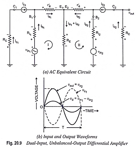
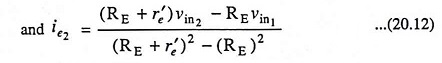
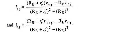
1. Voltage Gain: Applying KVL to loops I and II of the circuit given in Fig. 20.9 (a), we have
The above equations are the same as Eqs. (20.7) and (20.8), so the expressions for ie1 and ie2 will be the same as Eqs. (20.11) and (20.12). So
The output voltage is given by
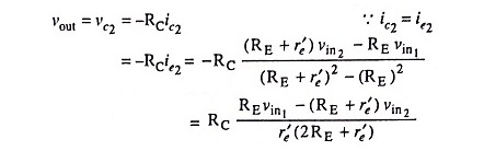
Usually r′e << RE; so (RE + r′e) ≡ RE and (2RE + r′e) ≡ 2RE.
Hence the equation for output voltage becomes
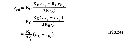
Voltage gain,
The above equation reveals that the voltage gain of the dual input unbalanced output differential amplifier is half the gain of dual-input, balanced-output differential amplifier [Eq. (20.15)].

The input and output waveforms of this amplifier are depicted in Fig. 20.9 (b). The noteworthy point is that in this configuration the dc voltage at the output terminal is the error voltage in the desired output signal. Hence to overcome this drawback this configuration is followed by a level translator circuit.
2. Differential Input Resistance: The two configurations of differential amplifiers given in Figs. 20.2 and 20.8 differ only in the manner in which output voltage is measured. Since the input resistance seen from either input is independent of the manner in which the output voltage is measured, the input resistance seen from either input source of the circuit depicted in Fig. 20.8 should be the same as that of the circuit depicted in Fig. 20.2. Thus
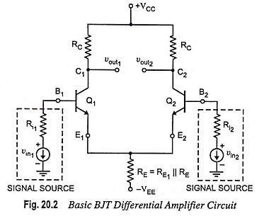
3. Output Resistance: The output resistance measured at collector C2 w.r.t. ground is equal to the collector resistance RC.
Thus
![]()
Output resistance,
![]()
Common-Mode Analysis:
The common-mode analysis of dual input unbalanced output differential amplifier is identical to that of common-mode analysis of dual-input, balanced-output differential amplifier i.e., common-mode gain,